
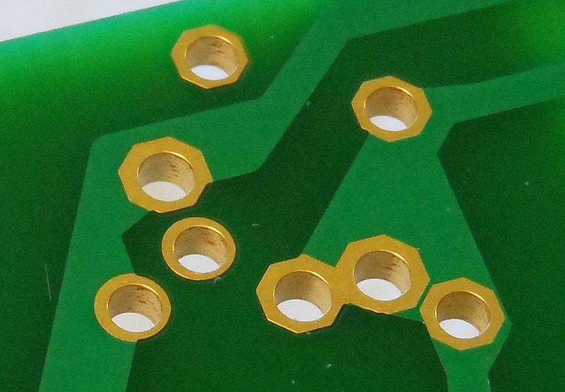
Image: Plated-through holes on an electronic circuit board

Size of this preview: 800 × 555 pixels. Other resolutions: 320 × 222 pixels | 1,180 × 818 pixels.
Original image (1,180 × 818 pixels, file size: 142 KB, MIME type: image/jpeg)
Description: Close-up view of an electronic printed circuit board showing plated-through holes (gold plated), circuit tracks (light green), and solder resist (a green ink printed over all the surface except for the gold patches and holes). The view shows about a 10mm width of the board, which is 1.6mm thick.
Title: Plated-through holes on an electronic circuit board
Credit: I took this photo using my own camera in my own home
Author: G1MFG
Usage Terms: Creative Commons Attribution-ShareAlike 4.0
License: CC-BY-SA-4.0
License Link: https://creativecommons.org/licenses/by-sa/4.0/
Attribution Required?: Yes
Image usage

All content from Kiddle encyclopedia articles (including the article images and facts) can be freely used under Attribution-ShareAlike license, unless stated otherwise.