
Photomask facts for kids

A photomask is like a super tiny stencil used to make electronic parts. Imagine you want to draw a very detailed picture, but you need to make hundreds or thousands of copies exactly the same. A photomask helps do just that for things like printed circuit boards and integrated circuits (computer chips).
It's a key tool in a process called photolithography. This process uses light to "draw" patterns onto special materials. Think of it like developing a photograph, but instead of a picture, you're making the tiny circuits that power our phones, computers, and other gadgets.
Contents
What is a Photomask?
A photomask is a flat piece of glass or quartz with a pattern on it. This pattern is made of a thin layer of metal, usually chrome. The metal blocks light, while the clear parts let light pass through. Each photomask holds the design for a specific layer of an electronic circuit.
How Photomasks Make Circuits
Making a computer chip or circuit board is a bit like building with super tiny LEGOs. You add layers, one by one. Here's how a photomask helps:
- First, a special material called a photoresist is put on a silicon wafer (a thin slice of silicon, like a very smooth disc).
- Then, the photomask is placed over the wafer.
- Next, light shines through the photomask. The light goes through the clear parts of the mask and hits the photoresist below. The metal parts of the mask block the light.
- Where the light hits, the photoresist changes. It becomes either harder or softer, depending on the type of photoresist.
- After the light step, the wafer is put into a special liquid, like a developer. This liquid washes away either the parts of the photoresist that were hit by light or the parts that were not.
- Now, the wafer has the circuit pattern etched into the photoresist. The parts of the silicon wafer that are not covered by the photoresist can then be changed, for example, by adding or removing material.
- This process is repeated many times, with different photomasks, to build up all the complex layers of a computer chip.
Types of Photomasks
There are a few main types of photomasks, each with its own benefits.
Contact Masks
- How they work: These masks actually touch the silicon wafer.
- Pros: They are generally cheaper to make.
- Cons: Because they touch the wafer, they can get damaged more easily. They also aren't as precise, meaning the patterns they create might not be as sharp or tiny.
Proximity Masks
- How they work: These masks are placed very close to the wafer, but they don't touch it. There's a tiny gap between the mask and the wafer.
- Pros: Since they don't touch, they last longer and are less likely to get damaged. They are also much more precise than contact masks, allowing for smaller and more detailed circuit patterns.
- Cons: They are more expensive to produce because of the higher precision needed.
Projection Masks (Reticles)
- How they work: These masks don't cover the whole wafer at once. Instead, they only contain the pattern for one single chip. A special lens system then projects this pattern onto the wafer, shrinking it down. The wafer is moved, and the pattern is projected again and again to create many chips on one wafer.
- Pros: They are extremely precise and can create incredibly tiny features, which is essential for modern, powerful computer chips.
- Cons: They are the most expensive type of mask due to the complex technology involved.
Photomasks are a crucial part of making almost all modern electronics. Without them, we wouldn't have the tiny, powerful chips that make our digital world possible!
Images for kids
-
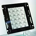
A photomask
-
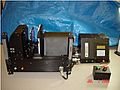
Pellicle Mounting Machine MLI


See also
 In Spanish: Máscara fotográfica para niños
