
Printed circuit board facts for kids

A printed circuit board (often called a PCB) is a special board that connects electronic parts. You can find PCBs in almost all computers and electronic devices today. Think of them as the "brain" or "nervous system" of your gadgets!
PCBs are usually made from a material that doesn't let electricity pass through it, like fiberglass. Thin lines of copper are etched onto or inside the board. These copper lines act like tiny wires, guiding electricity exactly where it needs to go.
Electronic parts are then attached to the PCB. They use a metal to connect to the copper lines. This lets electricity flow from one part to another, creating an electrical circuit.
Many different parts can be connected on a PCB to work together. Most PCBs are made for a specific job. For example, they help run your computer, cell phone, or television. Some PCBs are sold blank, so people can build their own custom electronic projects. Most things that use electricity have at least one PCB inside them to make them work.
Some PCBs are made to be flexible, meaning they can bend. These are called flexible circuit boards. There are also "rigid-flex" boards. These combine hard parts with bendable parts.
Contents
How Printed Circuit Boards Started

Printed circuit boards have a long history. The first ideas for connecting electrical parts came about in the 1850s. Back then, people used metal strips or rods to connect big electrical parts on wooden bases.
Later, wires replaced the metal strips. Wooden bases were swapped for metal frames. This helped make things smaller, which was important as circuits became more complex.
In 1913, Arthur Berry in Britain got a patent for a "print-and-etch" method. Then, in 1925, Charles Ducas in the United States created a new way to make electrical paths. He used a special ink that could conduct electricity. He printed this ink directly onto a surface that didn't conduct electricity. He called this "printed wiring" or "printed circuit."
A big step forward happened in 1943. Paul Eisler, an Austrian working in the United Kingdom, patented a method. He etched patterns of copper onto a hard, non-conductive base. The US military noticed Eisler's idea. They started using it in new weapons during World War II, like proximity fuzes.
Eisler's idea became very important in the 1950s. This was when the transistor was invented. Before transistors, parts like vacuum tubes were very large. Traditional wiring methods worked fine. But transistors were tiny! Manufacturers needed PCBs so the connections could also be small.
In 1961, a US company called Hazeltine patented "plated through-hole technology." This allowed for much more complex PCBs with many layers. Parts could be placed very close together. In the 1970s, Integrated circuit chips came along. These chips were quickly used in PCB designs. Today, some PCBs can have up to 100 layers!
Another important invention was Surface-mount technology. It was developed in the 1960s. This technology became very popular in the late 1980s.
Designing a Printed Circuit Board
The main job in designing a PCB is figuring out where all the electronic parts will go. Usually, a plan or diagram (called a schematic) is turned into a PCB design. There isn't one standard PCB. Each board is designed for its own specific use. It must also be the right size to fit where it's needed.
Designers use special computer software to plan the circuits on the board. The tiny spaces between electrical paths can be very small, sometimes less than 0.04 inches (1.0 mm). The software also plans where holes for parts or contact points will be.
Once the circuit pattern is ready, a negative image is printed. This image is printed at the exact size onto a clear plastic sheet. In a negative image, the areas that are *not* part of the circuit are black. The circuit pattern itself is clear. This design then guides machines to remove unwanted metal, usually with chemicals. It also guides drilling machines or automatic solder paste machines during manufacturing.
How Printed Circuit Boards Are Made
PCBs are made with outer layers of copper. The unwanted copper is removed, leaving behind the copper "wires." These wires will connect the electronic parts. The parts are then placed onto the board, making contact with these wires.
Using Photoresist
One way to make circuit boards is with photolithography. A special coating called photoresist is put on the board. This coating reacts to light. Then, the board and its coating are put into a developer liquid. This method can be expensive for each board. However, it is very cheap to set up at the beginning.
Using Silkscreen Printing
Another way to make PCBs is using a process called silk screen printing. In this method, a cloth is stretched tightly over a frame. An image of the circuit is printed onto this cloth. Then, ink is pushed through the cloth. The ink does not go where the image was printed. This method is called silk-screening because silk cloth is often used. Silk has very tiny holes, which is perfect for this job.
Silk-screening is used to print a special ink called "resist" onto the board. This resist ink protects the copper from an "etchant." An etchant is a chemical that dissolves copper. So, the etchant removes the copper that is *not* covered by the resist ink. This method is cheaper per board than photoresist. But it costs more to set up at the start.
Using a Mill
A third way to make a circuit board is by using a mill. A mill is like a drill that can move in many directions. The mill removes small amounts of copper each time it moves across the board. It removes the copper around the wires on the board. This leaves the copper wires in place. Other methods remove the extra copper differently.
This milling method is cheaper for each board. However, the equipment to make it is expensive. This method is not used as often as the other two. The other two methods are usually easier.
Images for kids
-
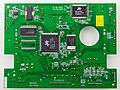
PCB of a DVD player. PCBs may be made in other colors.
-
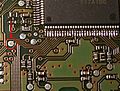
Part of a 1984 Sinclair ZX Spectrum computer board, a PCB, showing the conductive traces, vias (the through-hole paths to the other surface), and some electronic components mounted using through-hole mounting.
-
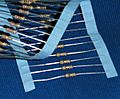
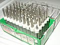
Through-hole (leaded) resistors
-
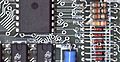
Surface mount components, including resistors, transistors and an integrated circuit
-
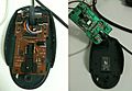
A PCB in a computer mouse: the component side (left) and the printed side (right)
-
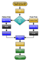
The two processing methods used to produce a double-sided PWB with plated-through holes
-
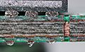
Cut through a SDRAM-module, a multi-layer PCB. Note the via, visible as a bright copper-colored band running between the top and bottom layers of the board.
-
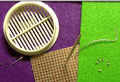
Eyelets (hollow)
-
PCB with test connection pads
-
A cordwood module
-
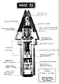
Cordwood construction was used in proximity fuzes.
-
Proximity fuze Mark 53 production line 1944
-
An example of hand-drawn etched traces on a PCB
-
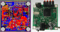
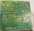
A PCB as a design on a computer (left) and realized as a board assembly populated with components (right). The board is double sided, with through-hole plating, green solder resist and a white legend. Both surface mount and through-hole components have been used.
-
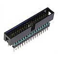
A breakout board can allow interconnection between two incompatible connectors.
-
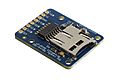
This breakout board allows an SD card's pins to be accessed easily while still allowing the card to be hot-swapped.
-
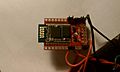
A breakout board allows a module (a Bluetooth module in this case) to have larger pins.
-
title=}}


.jpg)


See also
 In Spanish: Circuito impreso para niños
