
MOSFET facts for kids

A MOSFET is a tiny electronic component that works like an electrically-controlled switch.
MOSFET stands for metal-oxide-semiconductor field-effect transistor. These small devices are super important in modern electronics. You can find them in things like alarm clocks, calculators, and especially computers. They are like the basic building blocks that make many electronic gadgets work. Some MOSFETs help make analog signals stronger or process them, but most are used in digital electronics, which deals with on/off signals.
Think of a MOSFET as a special kind of valve for electricity. It has three main connections:
- The "gate" is like the control knob or switch.
- The "source" is where electricity enters.
- The "drain" is where electricity leaves.
The gate acts as a switch that controls the flow of electricity between the source and the drain. Imagine a water faucet: the handle is the "gate," the water coming from the pipe is the "source," and the water flowing out of the faucet is the "drain." By turning the handle (the gate), you control how much water (electricity) flows.
The name MOSFET tells us how it's built and what it does. "MOS" means it's made by layering different materials:
- Metal (the gate)
- Oxide (an insulator that stops electricity from flowing)
- Semiconductor (the source and drain, which can conduct electricity)
"FET" describes how the gate controls the semiconductor. When an electric signal is sent to the gate, it creates an electric field. This field changes how the source and drain are connected, allowing electricity to flow or stopping it.
Most MOSFETs are found inside integrated circuits, also known as computer chips. These chips are incredibly small, but they can hold billions of tiny transistors. For example, in 2008, a single chip could have 2,000,000,000 (2 billion!) transistors. Back in 1970, a chip could only hold about 2,000. This shows how much technology has grown!
Contents
How Do MOSFETs Work?
There are four main types of MOSFETs, and they each work a little differently. They control whether the switch between the "source" and "drain" is normally on or off, and what kind of voltage you need to apply to the gate to change it.
Enhancement Mode N-Channel MOSFET
- Normally: The switch between the source and drain is usually off.
- To turn on: You need to apply a positive voltage to the gate. This voltage must be higher than the voltage at the source.
Enhancement Mode P-Channel MOSFET
- Normally: The switch between the source and drain is usually off.
- To turn on: You need to apply a negative voltage to the gate. This voltage must be lower than the voltage at the source.
Depletion Mode N-Channel MOSFET
- Normally: The switch between the source and drain is usually on.
- To turn off: You need to apply a negative voltage to the gate. This voltage must be lower than the voltage at the source.
Depletion Mode P-Channel MOSFET
- Normally: The switch between the source and drain is usually on.
- To turn off: You need to apply a positive voltage to the gate. This voltage must be higher than the voltage at the source.
Depletion mode P-Channel MOSFETs are not very common.
Quick Summary of MOSFET Types
| MOSFET Type | Normally | To change, apply ____ voltage to the "gate" |
|---|---|---|
| Enhancement mode N-Channel | Off | Positive |
| Enhancement mode P-Channel | Off | Negative |
| Depletion mode N-Channel | On | Negative |
| Depletion mode P-Channel | On | Positive |
Why Are MOSFETs Different?
Tiny Integrated Circuits
Millions of MOSFETs can be made on a small piece of silicon. This creates an integrated circuit, which is the brain of many electronic devices. You can learn more about them in the integrated circuit article.
Dealing with Heat
When a MOSFET is working, especially if it's partly on, it can turn some of the electrical power into heat. Even when it's fully on, a small amount of power is still lost as heat.
This happens because the MOSFET has a small amount of resistance. When electricity flows through it, there's a tiny drop in voltage. This lost power becomes heat.
MOSFETs need to get rid of this heat, usually by releasing it into the air. Smaller MOSFETs might just warm up the air around them. Larger, more powerful MOSFETs often need a special metal part called a heatsink. A heatsink has fins that help spread the heat over a larger area, allowing it to cool down faster. Sometimes, a fan is even needed to blow air over the heatsink for extra cooling.
Other Important Differences
There are many different kinds of MOSFETs, each designed for specific jobs. When engineers choose a MOSFET for a project, they look at several things:
- Voltage limits: How much voltage the gate or the main path (drain to source) can handle without breaking.
- Current limits: How much electricity can flow through it. If you need to power something big like a motor, you'll need a MOSFET that can handle high currents.
- Switching speed: How fast the MOSFET can turn on and off. Some are super fast, perfect for computers, while others are slower but can handle more power.
- Static electricity: Static electricity can easily damage a MOSFET. Some MOSFETs have built-in protection against it.
- Multiple MOSFETs: Sometimes, several MOSFETs are put together in one single device. This makes the electronic circuit board smaller and can be cheaper to build.
How MOSFETs Are Made

MOSFETs are built using special materials called semiconductors, usually silicon. In silicon, there are two main types:
- P-type silicon: This has "holes," which are like empty spaces that attract electrons.
- N-type silicon: This has extra electrons.
When P-type and N-type silicon meet, they form a "junction." At this junction, a "depletion region" forms. This is an area where there are no free electrons or holes, so electricity can't easily flow through it.
MOSFETs use this depletion region to their advantage. When a positive voltage is applied to the "gate," it creates a small electric field. This field can temporarily remove the depletion region directly under the gate, creating a path called an "N-Channel." This N-Channel allows electrons from the "source" to flow easily to the "drain," turning the MOSFET switch "on."
Images for kids
-
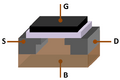
MOSFET showing gate (G), body (B), source (S) and drain (D) terminals. The gate is separated from the body by an insulating layer (pink).
-
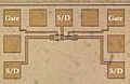
Photomicrograph of two metal-gate MOSFETs in a test pattern. Probe pads for two gates and three source/drain nodes are labeled.
-
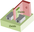
A FinFET


See also
 In Spanish: Transistor de efecto de campo metal-óxido-semiconductor para niños
