Operational amplifier facts for kids
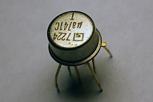
The μA741, a popular early integrated op amp
|
|
Type | Discrete circuit Integrated circuit |
---|---|
Invented | Karl D. Swartzel Jr. |
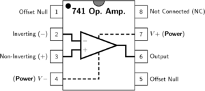
Pin configuration |
|
Electronic symbol | |
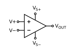
Circuit diagram symbol for a representative op amp. Pins are labeled as listed above. |
An operational amplifier (often op amp or opamp) is a DC-coupled high-gain electronic voltage amplifier with a differential input and, usually, a single-ended output. In this configuration, an op amp produces an output potential (relative to circuit ground) that is typically 100,000 times larger than the potential difference between its input terminals. The operational amplifier traces its origin and name to analog computers, where they were used to perform mathematical operations in linear, non-linear, and frequency-dependent circuits.
The popularity of the op amp as a building block in analog circuits is due to its versatility. By using negative feedback, the characteristics of an op-amp circuit, its gain, input and output impedance, bandwidth etc. are determined by external components and have little dependence on temperature coefficients or engineering tolerance in the op amp itself.
Op amps are used widely in electronic devices today, including a vast array of consumer, industrial, and scientific devices. Many standard integrated circuit op amps cost only a few cents; however, some integrated or hybrid operational amplifiers with special performance specifications may cost over US$100 in small quantities. Op amps may be packaged as components or used as elements of more complex integrated circuits.
The op amp is one type of differential amplifier. Other types of differential amplifier include the fully differential amplifier (an op amp with a differential rather than single-ended output), the instrumentation amplifier (usually built from three op amps), the isolation amplifier (with galvanic isolation between input and output), and negative-feedback amplifier (usually built from one or more op amps and a resistive feedback network).
Contents
Operation
The amplifier's differential inputs consist of a non-inverting input (+) with voltage V+ and an inverting input (−) with voltage V−; ideally the op amp amplifies only the difference in voltage between the two, which is called the differential input voltage. The output voltage of the op amp Vout is given by the equation
where AOL is the open-loop gain of the amplifier (the term "open-loop" refers to the absence of an external feedback loop from the output to the input).
Open-loop amplifier
The magnitude of AOL is typically very large (100,000 or more for integrated circuit op amps), and therefore even a quite small difference between V+ and V− drives the amplifier into clipping or saturation. The magnitude of AOL is not well controlled by the manufacturing process, and so it is impractical to use an open-loop amplifier as a stand-alone differential amplifier.
Without negative feedback, and optionally positive feedback for regeneration, an op amp acts as a comparator. If the inverting input is held at ground (0 V), and the input voltage Vin applied to the non-inverting input is positive, the output will be maximum positive; if Vin is negative, the output will be maximum negative. Because there is no feedback from the output to either input, this is an open-loop circuit acting as a comparator.
Closed-loop amplifier
If predictable operation is desired, negative feedback is used, by applying a portion of the output voltage to the inverting input. The closed-loop feedback greatly reduces the gain of the circuit. When negative feedback is used, the circuit's overall gain and response is determined primarily by the feedback network, rather than by the op-amp characteristics. If the feedback network is made of components with values small relative to the op amp's input impedance, the value of the op amp's open-loop response AOL does not seriously affect the circuit's performance. In this context, high input impedance at the input terminals and low output impedance at the output terminal(s) are particularly useful features of an op amp.
The response of the op-amp circuit with its input, output, and feedback circuits to an input is characterized mathematically by a transfer function; designing an op-amp circuit to have a desired transfer function is in the realm of electrical engineering. The transfer functions are important in most applications of op amps, such as in analog computers.
In the non-inverting amplifier on the right, the presence of negative feedback via the voltage divider Rf, Rg determines the closed-loop gain ACL = Vout / Vin. Equilibrium will be established when Vout is just sufficient to pull the inverting input to the same voltage as Vin. The voltage gain of the entire circuit is thus 1 + Rf / Rg. As a simple example, if Vin = 1 V and Rf = Rg, Vout will be 2 V, exactly the amount required to keep V− at 1 V. Because of the feedback provided by the Rf, Rg network, this is a closed-loop circuit.
Another way to analyze this circuit proceeds by making the following (usually valid) assumptions:
- When an op amp operates in linear (i.e., not saturated) mode, the difference in voltage between the non-inverting (+) and inverting (−) pins is negligibly small.
- The input impedance of the (+) and (−) pins is much larger than other resistances in the circuit.
The input signal Vin appears at both (+) and (−) pins per assumption 1, resulting in a current i through Rg equal to Vin / Rg:
Since Kirchhoff's current law states that the same current must leave a node as enter it, and since the impedance into the (−) pin is near infinity per assumption 2, we can assume practically all of the same current i flows through Rf, creating an output voltage
By combining terms, we determine the closed-loop gain ACL:
Op-amp characteristics
Ideal op amps
An ideal op amp is usually considered to have the following characteristics:
- Infinite open-loop gain G = vout / vin
- Infinite input impedance Rin, and so zero input current
- Zero input offset voltage
- Infinite output voltage range
- Infinite bandwidth with zero phase shift and infinite slew rate
- Zero output impedance Rout, and so infinite output current range
- Zero noise
- Infinite common-mode rejection ratio (CMRR)
- Infinite power supply rejection ratio.
These ideals can be summarized by the two golden rules:
- In a closed loop the output does whatever is necessary to make the voltage difference between the inputs zero.
- The inputs draw zero current.
The first rule only applies in the usual case where the op amp is used in a closed-loop design (negative feedback, where there is a signal path of some sort feeding back from the output to the inverting input). These rules are commonly used as a good first approximation for analyzing or designing op-amp circuits.
None of these ideals can be perfectly realized. A real op amp may be modeled with non-infinite or non-zero parameters using equivalent resistors and capacitors in the op-amp model. The designer can then include these effects into the overall performance of the final circuit. Some parameters may turn out to have negligible effect on the final design while others represent actual limitations of the final performance.
Real op amps
Real op amps differ from the ideal model in various aspects.
- Finite gain
- Open-loop gain is finite in real operational amplifiers. Typical devices exhibit open-loop DC gain exceeding 100,000. So long as the loop gain (i.e., the product of open-loop and feedback gains) is very large, the closed-loop gain will be determined entirely by the amount of negative feedback (i.e., it will be independent of open-loop gain). In applications where the closed-loop gain must be very high (approaching the open-loop gain), the feedback gain will be very low and the lower loop gain in these cases causes non-ideal behavior from the circuit.
- Non-zero output impedance
- Low output impedance is important for low-impedance loads; for these loads, the voltage drop across the output impedance effectively reduces the open-loop gain. In configurations with a voltage-sensing negative feedback, the output impedance of the amplifier is effectively lowered; thus, in linear applications, op-amp circuits usually exhibit a very low output impedance.
- Low-impedance outputs typically require high quiescent (i.e., idle) current in the output stage and will dissipate more power, so low-power designs may purposely sacrifice low output impedance.
- Finite input impedances
- The differential input impedance of the operational amplifier is defined as the impedance between its two inputs; the common-mode input impedance is the impedance from each input to ground. MOSFET-input operational amplifiers often have protection circuits that effectively short circuit any input differences greater than a small threshold, so the input impedance can appear to be very low in some tests. However, as long as these operational amplifiers are used in a typical high-gain negative feedback application, these protection circuits will be inactive. The input bias and leakage currents described below are a more important design parameter for typical operational amplifier applications.
- Input capacitance
- Additional input impedance due to parasitic capacitance can be a critical issue for high-frequency operation where it reduces input impedance and may cause phase shifts.
- Input current
- Due to biasing requirements or leakage, a small amount of current flows into the inputs. When high resistances or sources with high output impedances are used in the circuit, these small currents can produce voltage drops. If the input currents are matched, and the impedance looking out of both inputs are matched, then the voltages produced at each input will be equal. Because the operational amplifier operates on the difference between its inputs, these matched voltages will have no effect. It is more common for the input currents to be slightly mismatched. The difference is called input offset current, and even with matched resistances a small offset voltage (distinct from the input offset voltage below) can be produced. This offset voltage can create offsets or drifting in the operational amplifier.
- Input offset voltage
- Voltage required across the op amp's input terminals to drive the output voltage to zero. In the perfect amplifier, there would be no input offset voltage. However, it exists because of imperfections in the differential amplifier input stage of op amps. Input offset voltage creates two problems: First, due to the amplifier's high voltage gain, it virtually assures that the amplifier output will go into saturation if it is operated without negative feedback, even when the input terminals are wired together. Second, in a closed loop, negative feedback configuration, the input offset voltage is amplified along with the signal and this may pose a problem if high precision DC amplification is required or if the input signal is very small.
- Common-mode gain
- A perfect operational amplifier amplifies only the voltage difference between its two inputs, completely rejecting all voltages that are common to both. However, the differential input stage of an operational amplifier is never perfect, leading to the amplification of these common voltages to some degree. The standard measure of this defect is called the common-mode rejection ratio (CMRR). Minimization of common-mode gain is important in non-inverting amplifiers that operate at high gain.
- Power-supply rejection
- The output of a perfect operational amplifier will be independent of power supply voltage fluctuations. Every real operational amplifier has a finite power supply rejection ratio (PSRR) that reflects how well the op amp can reject noise in its power supply from propagating to the output. With increasing frequency the power-supply rejection usually gets worse.
- Temperature effects
- Performance and properties of the amplifier typically changes, to some extent, with changes in temperature. Temperature drift of the input offset voltage is especially important.
- Drift
- Real op-amp parameters are subject to slow change over time and with changes in temperature, input conditions, etc.
- Finite bandwidth
- All amplifiers have finite bandwidth. To a first approximation, the op amp has the frequency response of an integrator with gain. That is, the gain of a typical op amp is inversely proportional to frequency and is characterized by its gain–bandwidth product (GBWP). For example, an op amp with a GBWP of 1 MHz would have a gain of 5 at 200 kHz, and a gain of 1 at 1 MHz. This dynamic response coupled with the very high DC gain of the op amp gives it the characteristics of a first-order low-pass filter with very high DC gain and low cutoff frequency given by the GBWP divided by the DC gain.
The finite bandwidth of an op amp can be the source of several problems, including:
- Stability
- Associated with the bandwidth limitation is a phase difference between the input signal and the amplifier output that can lead to oscillation in some feedback circuits. For example, a sinusoidal output signal meant to interfere destructively with an input signal of the same frequency will interfere constructively if delayed by 180 degrees forming positive feedback. In these cases, the feedback circuit can be stabilized by means of frequency compensation, which increases the gain or phase margin of the open-loop circuit. The circuit designer can implement this compensation externally with a separate circuit component. Alternatively, the compensation can be implemented within the operational amplifier with the addition of a dominant pole that sufficiently attenuates the high-frequency gain of the operational amplifier. The location of this pole may be fixed internally by the manufacturer or configured by the circuit designer using methods specific to the op amp. In general, dominant-pole frequency compensation reduces the bandwidth of the op amp even further. When the desired closed-loop gain is high, op-amp frequency compensation is often not needed because the requisite open-loop gain is sufficiently low; consequently, applications with high closed-loop gain can make use of op amps with higher bandwidths.
- Distortion, and other effects
- Limited bandwidth also results in lower amounts of feedback at higher frequencies, producing higher distortion, and output impedance as the frequency increases.
- Noise
- Amplifiers intrinsically output noise, even when there is no signal applied. This can be due to internal thermal noise and flicker noise of the device. For applications with high gain or high bandwidth, noise becomes an important consideration and a low-noise amplifier, which is specifically designed for minimum intrinsic noise, may be required to meet performance requirements.
Non-linear imperfections
- Saturation
- Output voltage is limited to a minimum and maximum value close to the power supply voltages. The output of older op amps can reach to within one or two volts of the supply rails. The output of so-called rail-to-rail op amps can reach to within millivolts of the supply rails when providing low output currents.
- Slew rate limiting
- The amplifier's output voltage reaches its maximum rate of change, the slew rate, usually specified in volts per microsecond (V/μs). When slew rate limiting occurs, further increases in the input signal have no effect on the rate of change of the output. Slew rate limiting is usually caused by the input stage saturating; the result is a constant current i driving a capacitance C in the amplifier (especially those capacitances used to implement its frequency compensation); the slew rate is limited by dv/dt = i/C. Slewing is associated with the large-signal performance of an op amp. Consider, for example, an op amp configured for a gain of 10. Let the input be a 1 V, 100 kHz sawtooth wave. That is, the amplitude is 1 V and the period is 10 microseconds. Accordingly, the rate of change (i.e., the slope) of the input is 0.1 V per microsecond. After 10× amplification, the output should be a 10 V, 100 kHz sawtooth, with a corresponding slew rate of 1 V per microsecond. However, the classic 741 op amp has a 0.5 V per microsecond slew rate specification so that its output can rise to no more than 5 V in the sawtooth's 10-microsecond period. Thus, if one were to measure the output, it would be a 5 V, 100 kHz sawtooth, rather than a 10 V, 100 kHz sawtooth. Next consider the same amplifier and 100 kHz sawtooth, but now the input amplitude is 100 mV rather than 1 V. After 10× amplification the output is a 1 V, 100 kHz sawtooth with a corresponding slew rate of 0.1 V per microsecond. In this instance, the 741 with its 0.5 V per microsecond slew rate will amplify the input properly. Modern high-speed op amps can have slew rates in excess of 5,000 V per microsecond. However, it is more common for op amps to have slew rates in the range 5–100 V per microsecond. For example, the general purpose TL081 op amp has a slew rate of 13 V per microsecond. As a general rule, low power and small bandwidth op amps have low slew rates. As an example, the LT1494 micropower op amp consumes 1.5 microamp but has a 2.7 kHz gain-bandwidth product and a 0.001 V per microsecond slew rate.
- Non-linear input-output relationship
- The output voltage may not be accurately proportional to the difference between the input voltages producing distortion. This effect will be very small in a practical circuit where substantial negative feedback is used.
- Phase reversal
- In some integrated op amps, when the published common mode voltage is violated (e.g., by one of the inputs being driven to one of the supply voltages), the output may slew to the opposite polarity from what is expected in normal operation. Under such conditions, negative feedback becomes positive, likely causing the circuit to lock up in that state.
Power considerations
- Limited output current
- The output current must be finite. In practice, most op amps are designed to limit the output current to prevent damage to the device, typically around 25 mA for a type 741 IC op amp. Modern designs are electronically more robust than earlier implementations and some can sustain direct short circuits on their outputs without damage.
- Limited output voltage
- Output voltage cannot exceed the power supply voltage supplied to the op amp. The maximum output of most op amps is further reduced by some amount due to limitations in the output circuitry. Rail-to-rail op amps are designed for maximum output levels.
- Output sink current
- The output sink current is the maximum current allowed to sink into the output stage. Some manufacturers provide an output voltage vs. the output sink current plot which gives an idea of the output voltage when it is sinking current from another source into the output pin.
- Limited dissipated power
- The output current flows through the op amp's internal output impedance, generating heat that must be dissipated. If the op amp dissipates too much power, then its temperature will increase above some safe limit. The op amp must shut down or risk being damaged.
Modern integrated FET or MOSFET op amps approximate more closely the ideal op amp than bipolar ICs when it comes to input impedance and input bias currents. Bipolars are generally better when it comes to input voltage offset, and often have lower noise. Generally, at room temperature, with a fairly large signal, and limited bandwidth, FET and MOSFET op amps now offer better performance.
Internal circuitry of 741-type op amp
Sourced by many manufacturers, and in multiple similar products, an example of a bipolar transistor operational amplifier is the 741 integrated circuit designed in 1968 by David Fullagar at Fairchild Semiconductor after Bob Widlar's LM301 integrated circuit design. In this discussion, we use the parameters of the hybrid-pi model to characterize the small-signal, grounded emitter characteristics of a transistor. In this model, the current gain of a transistor is denoted hfe, more commonly called the β.
Architecture
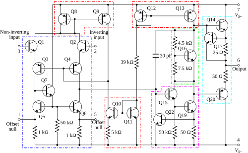
A small-scale integrated circuit, the 741 op amp shares with most op amps an internal structure consisting of three gain stages:
- Differential amplifier (outlined dark blue) — provides high differential amplification (gain), with rejection of common-mode signal, low noise, high input impedance, and drives a
- Voltage amplifier (outlined magenta) — provides high voltage gain, a single-pole frequency roll-off, and in turn drives the
- Output amplifier (outlined cyan and green) — provides high current gain (low output impedance), along with output current limiting, and output short-circuit protection.
Additionally, it contains current mirror (outlined red) bias circuitry and compensation capacitor (30 pF).
Differential amplifier
The input stage consists of a cascaded differential amplifier (outlined in dark blue) followed by a current-mirror active load. This constitutes a transconductance amplifier, turning a differential voltage signal at the bases of Q1, Q2 into a current signal into the base of Q15.
It entails two cascaded transistor pairs, satisfying conflicting requirements. The first stage consists of the matched NPN emitter follower pair Q1, Q2 that provide high input impedance. The second is the matched PNP common-base pair Q3, Q4 that eliminates the undesirable Miller effect; it drives an active load Q7 plus matched pair Q5, Q6.
That active load is implemented as a modified Wilson current mirror; its role is to convert the (differential) input current signal to a single-ended signal without the attendant 50% losses (increasing the op amp's open-loop gain by 3 dB). Thus, a small-signal differential current in Q3 versus Q4 appears summed (doubled) at the base of Q15, the input of the voltage gain stage.
Voltage amplifier
The (class-A) voltage gain stage (outlined in magenta) consists of the two NPN transistors Q15 and Q19 connected in a Darlington configuration and uses the output side of current mirror formed by Q12 and Q13 as its collector (dynamic) load to achieve its high voltage gain. The output sink transistor Q20 receives its base drive from the common collectors of Q15 and Q19; the level-shifter Q16 provides base drive for the output source transistor Q14. The transistor Q22 prevents this stage from delivering excessive current to Q20 and thus limits the output sink current.
Output amplifier
The output stage (Q14, Q20, outlined in cyan) is a Class AB amplifier. It provides an output drive with impedance of ~50 Ω, in essence, current gain. Transistor Q16 (outlined in green) provides the quiescent current for the output transistors and Q17 limits output source current.
Biasing circuits
Biasing circuits provide appropriate quiescent current for each stage of the op amp.
The resistor (39 kΩ) connecting the (diode-connected) Q11 and Q12, and the given supply voltage (VS+ − VS−), determine the current in the current mirrors, (matched pairs) Q10/Q11 and Q12/Q13. The collector current of Q11, i11 × 39 kΩ = VS+ − VS− − 2 VBE. For the typical VS = ±20 V, the standing current in Q11/Q12 (as well as in Q13) would be ~1 mA. A supply current for a typical 741 of about 2 mA agrees with the notion that these two bias currents dominate the quiescent supply current.
Transistors Q11 and Q10 form a Widlar current mirror, with quiescent current in Q10 i10 such that ln(i11 / i10) = i10 × 5 kΩ / 28 mV, where 5 kΩ represents the emitter resistor of Q10, and 28 mV is VT, the thermal voltage at room temperature. In this case i10 ≈ 20 μA.
Differential amplifier
The biasing circuit of this stage is set by a feedback loop that forces the collector currents of Q10 and Q9 to (nearly) match. The small difference in these currents provides the drive for the common base of Q3/Q4 (note that the base drive for input transistors Q1/Q2 is the input bias current and must be sourced externally). The summed quiescent currents of Q1/Q3 plus Q2/Q4 is mirrored from Q8 into Q9, where it is summed with the collector current in Q10, the result being applied to the bases of Q3/Q4.
The quiescent currents of Q1/Q3 (resp., Q2/Q4) i1 will thus be half of i10, of order ~10 μA. Input bias current for the base of Q1 (resp. Q2) will amount to i1 / β; typically ~50 nA, implying a current gain hfe ≈ 200 for Q1(Q2).
This feedback circuit tends to draw the common base node of Q3/Q4 to a voltage Vcom − 2 VBE, where Vcom is the input common-mode voltage. At the same time, the magnitude of the quiescent current is relatively insensitive to the characteristics of the components Q1–Q4, such as hfe, that would otherwise cause temperature dependence or part-to-part variations.
Transistor Q7 drives Q5 and Q6 into conduction until their (equal) collector currents match that of Q1/Q3 and Q2/Q4. The quiescent current in Q7 is VBE / 50 kΩ, about 35 μA, as is the quiescent current in Q15, with its matching operating point. Thus, the quiescent currents are pairwise matched in Q1/Q2, Q3/Q4, Q5/Q6, and Q7/Q15.
Voltage amplifier
Quiescent currents in Q16 and Q19 are set by the current mirror Q12/Q13, which is running at ~1 mA. Through some mechanism, the collector current in Q19 tracks that standing current.
Output amplifier
In the circuit involving Q16 (variously named rubber diode or VBE multiplier), the 4.5 kΩ resistor must be conducting about 100 μA, with the Q16 VBE roughly 700 mV. Then the VCB must be about 0.45 V and VCE at about 1.0 V. Because the Q16 collector is driven by a current source and the Q16 emitter drives into the Q19 collector current sink, the Q16 transistor establishes a voltage difference between Q14 base and Q20 base of ~1 V, regardless of the common-mode voltage of Q14/Q20 base. The standing current in Q14/Q20 will be a factor exp(100 mV / VT) ≈ 36 smaller than the 1 mA quiescent current in the class A portion of the op amp. This (small) standing current in the output transistors establishes the output stage in class AB operation and reduces the crossover distortion of this stage.
Small-signal differential mode
A small differential input voltage signal gives rise, through multiple stages of current amplification, to a much larger voltage signal on output.
Input impedance
The input stage with Q1 and Q3 is similar to an emitter-coupled pair (long-tailed pair), with Q2 and Q4 adding some degenerating impedance. The input impedance is relatively high because of the small current through Q1-Q4. A typical 741 op amp has a differential input impedance of about 2 MΩ. The common mode input impedance is even higher, as the input stage works at an essentially constant current.
Differential amplifier
A differential voltage Vin at the op amp inputs (pins 3 and 2, respectively) gives rise to a small differential current in the bases of Q1 and Q2 iin ≈ Vin / (2hiehfe). This differential base current causes a change in the differential collector current in each leg by iinhfe. Introducing the transconductance of Q1, gm = hfe / hie, the (small-signal) current at the base of Q15 (the input of the voltage gain stage) is Vingm / 2.
This portion of the op amp cleverly changes a differential signal at the op amp inputs to a single-ended signal at the base of Q15, and in a way that avoids wastefully discarding the signal in either leg. To see how, notice that a small negative change in voltage at the inverting input (Q2 base) drives it out of conduction, and this incremental decrease in current passes directly from Q4 collector to its emitter, resulting in a decrease in base drive for Q15. On the other hand, a small positive change in voltage at the non-inverting input (Q1 base) drives this transistor into conduction, reflected in an increase in current at the collector of Q3. This current drives Q7 further into conduction, which turns on current mirror Q5/Q6. Thus, the increase in Q3 emitter current is mirrored in an increase in Q6 collector current; the increased collector currents shunts more from the collector node and results in a decrease in base drive current for Q15. Besides avoiding wasting 3 dB of gain here, this technique decreases common-mode gain and feedthrough of power supply noise.
Voltage amplifier
A current signal i at Q15's base gives rise to a current in Q19 of order iβ2 (the product of the hfe of each of Q15 and Q19, which are connected in a Darlington pair). This current signal develops a voltage at the bases of output transistors Q14/Q20 proportional to the hie of the respective transistor.
Output amplifier
Output transistors Q14 and Q20 are each configured as an emitter follower, so no voltage gain occurs there; instead, this stage provides current gain, equal to the hfe of Q14 (resp. Q20).
The output impedance is not zero, as it would be in an ideal op amp, but with negative feedback it approaches zero at low frequencies.
Overall open-loop voltage gain
The net open-loop small-signal voltage gain of the op amp involves the product of the current gain hfe of some 4 transistors. In practice, the voltage gain for a typical 741-style op amp is of order 200,000, and the current gain, the ratio of input impedance (~2−6 MΩ) to output impedance (~50 Ω) provides yet more (power) gain.
Other linear characteristics
Small-signal common mode gain
The ideal op amp has infinite common-mode rejection ratio, or zero common-mode gain.
In the present circuit, if the input voltages change in the same direction, the negative feedback makes Q3/Q4 base voltage follow (with 2 VBE below) the input voltage variations. Now the output part (Q10) of Q10-Q11 current mirror keeps up the common current through Q9/Q8 constant in spite of varying voltage. Q3/Q4 collector currents, and accordingly the output current at the base of Q15, remain unchanged.
In the typical 741 op amp, the common-mode rejection ratio is 90 dB, implying an open-loop common-mode voltage gain of about 6.
Frequency compensation
The innovation of the Fairchild μA741 was the introduction of frequency compensation via an on-chip (monolithic) capacitor, simplifying application of the op amp by eliminating the need for external components for this function. The 30 pF capacitor stabilizes the amplifier via Miller compensation and functions in a manner similar to an op-amp integrator circuit. Also known as dominant pole compensation because it introduces a pole that masks (dominates) the effects of other poles into the open loop frequency response; in a 741 op amp this pole can be as low as 10 Hz (where it causes a −3 dB loss of open loop voltage gain).
This internal compensation is provided to achieve unconditional stability of the amplifier in negative feedback configurations where the feedback network is non-reactive and the closed loop gain is unity or higher. In contrast, amplifiers requiring external compensation, such as the μA748, may require external compensation or closed-loop gains significantly higher than unity.
Input offset voltage
The "offset null" pins may be used to place external resistors (typically in the form of the two ends of a potentiometer, with the slider connected to VS–) in parallel with the emitter resistors of Q5 and Q6, to adjust the balance of the Q5/Q6 current mirror. The potentiometer is adjusted such that the output is null (midrange) when the inputs are shorted together.
Non-linear characteristics
Input breakdown voltage
The transistors Q3, Q4 help to increase the reverse VBE rating: the base-emitter junctions of the NPN transistors Q1 and Q2 break down at around 7 V, but the PNP transistors Q3 and Q4 have VBE breakdown voltages around 50 V.
Output-stage voltage swing and current limiting
Variations in the quiescent current with temperature, or between parts with the same type number, are common, so crossover distortion and quiescent current may be subject to significant variation.
The output range of the amplifier is about one volt less than the supply voltage, owing in part to VBE of the output transistors Q14 and Q20.
The 25 Ω resistor at the Q14 emitter, along with Q17, acts to limit Q14 current to about 25 mA; otherwise, Q17 conducts no current.
Current limiting for Q20 is performed in the voltage gain stage: Q22 senses the voltage across Q19's emitter resistor (50 Ω); as it turns on, it diminishes the drive current to Q15 base.
Later versions of this amplifier schematic may show a somewhat different method of output current limiting.
Applicability considerations
While the 741 was historically used in audio and other sensitive equipment, such use is now rare because of the improved noise performance of more modern op amps. Apart from generating noticeable hiss, 741s and other older op amps may have poor common-mode rejection ratios and so will often introduce cable-borne mains hum and other common-mode interference, such as switch 'clicks', into sensitive equipment.
The "741" has come to often mean a generic op-amp IC (such as μA741, LM301, 558, LM324, TBA221 — or a more modern replacement such as the TL071). The description of the 741 output stage is qualitatively similar for many other designs (that may have quite different input stages), except:
- Some devices (μA748, LM301, LM308) are not internally compensated (require an external capacitor from output to some point within the operational amplifier, if used in low closed-loop gain applications).
- Some modern devices have rail-to-rail output capability, meaning that the output can range from within a few millivolts of the positive supply voltage to within a few millivolts of the negative supply voltage.
Classification
Op amps may be classified by their construction:
- discrete, built from individual transistors or tubes/valves,
- hybrid, consisting of discrete and integrated components,
- full integrated circuits — most common, having displaced the former two due to low cost.
IC op amps may be classified in many ways, including:
- Device grade, including acceptable operating temperature ranges and other environmental or quality factors. For example: LM101, LM201, and LM301 refer to the military, industrial, and commercial versions of the same component. Military and industrial grade components offer better performance in harsh conditions than their commercial counterparts, but are sold at higher prices.
- Classification by package type may also affect environmental hardiness, as well as manufacturing options; DIP, and other through-hole packages are tending to be replaced by surface-mount devices.
- Classification by internal compensation: op amps may suffer from high frequency instability in some negative feedback circuits unless a small compensation capacitor modifies the phase and frequency responses. Op amps with a built-in capacitor are termed compensated, and allow circuits above some specified closed-loop gain to operate stably with no external capacitor. In particular, op amps that are stable even with a closed loop gain of 1 are called unity gain compensated.
- Single, dual and quad versions of many commercial op-amp IC are available, meaning 1, 2 or 4 operational amplifiers are included in the same package.
- Rail-to-rail input (and/or output) op amps can work with input (and/or output) signals very close to the power supply rails.
- CMOS op amps (such as the CA3140E) provide extremely high input resistances, higher than JFET-input op amps, which are normally higher than bipolar-input op amps.
- other varieties of op amp include programmable op amps (simply meaning the quiescent current, bandwidth and so on can be adjusted by an external resistor).
- manufacturers often tabulate their op amps according to purpose, such as low-noise pre-amplifiers, wide bandwidth amplifiers, and so on.
Applications
Use in electronics system design
The use of op amps as circuit blocks is much easier and clearer than specifying all their individual circuit elements (transistors, resistors, etc.), whether the amplifiers used are integrated or discrete circuits. In the first approximation op amps can be used as if they were ideal differential gain blocks; at a later stage limits can be placed on the acceptable range of parameters for each op amp.
Circuit design follows the same lines for all electronic circuits. A specification is drawn up governing what the circuit is required to do, with allowable limits. For example, the gain may be required to be 100 times, with a tolerance of 5% but drift of less than 1% in a specified temperature range; the input impedance not less than one megohm; etc.
A basic circuit is designed, often with the help of circuit modeling (on a computer). Specific commercially available op amps and other components are then chosen that meet the design criteria within the specified tolerances at acceptable cost. If not all criteria can be met, the specification may need to be modified.
A prototype is then built and tested; changes to meet or improve the specification, alter functionality, or reduce the cost, may be made.
Applications without using any feedback
That is, the op amp is being used as a voltage comparator. Note that a device designed primarily as a comparator may be better if, for instance, speed is important or a wide range of input voltages may be found, since such devices can quickly recover from full on or full off ("saturated") states.
A voltage level detector can be obtained if a reference voltage Vref is applied to one of the op amp's inputs. This means that the op amp is set up as a comparator to detect a positive voltage. If the voltage to be sensed, Ei, is applied to op amp's (+) input, the result is a noninverting positive-level detector: when Ei is above Vref, VO equals +Vsat; when Ei is below Vref, VO equals −Vsat. If Ei is applied to the inverting input, the circuit is an inverting positive-level detector: When Ei is above Vref, VO equals −Vsat.
A zero voltage level detector (Ei = 0) can convert, for example, the output of a sine-wave from a function generator into a variable-frequency square wave. If Ei is a sine wave, triangular wave, or wave of any other shape that is symmetrical around zero, the zero-crossing detector's output will be square. Zero-crossing detection may also be useful in triggering TRIACs at the best time to reduce mains interference and current spikes.
Positive-feedback applications
Another typical configuration of op amps is with positive feedback, which takes a fraction of the output signal back to the non-inverting input. An important application of it is the comparator with hysteresis, the Schmitt trigger. Some circuits may use positive feedback and negative feedback around the same amplifier, for example triangle-wave oscillators and active filters.
Because of the wide slew range and lack of positive feedback, the response of all the open-loop level detectors described above will be relatively slow. External overall positive feedback may be applied, but (unlike internal positive feedback that may be applied within the latter stages of a purpose-designed comparator) this markedly affects the accuracy of the zero-crossing detection point. Using a general-purpose op amp, for example, the frequency of Ei for the sine to square wave converter should probably be below 100 Hz.
Negative-feedback applications
Non-inverting amplifier
In a non-inverting amplifier, the output voltage changes in the same direction as the input voltage.
The gain equation for the op amp is
However, in this circuit V− is a function of Vout because of the negative feedback through the R1 R2 network. R1 and R2 form a voltage divider, and as V− is a high-impedance input, it does not load it appreciably. Consequently
where
Substituting this into the gain equation, we obtain
Solving for :
If is very large, this simplifies to
The non-inverting input of the operational amplifier needs a path for DC to ground; if the signal source does not supply a DC path, or if that source requires a given load impedance, then the circuit will require another resistor from the non-inverting input to ground. When the operational amplifier's input bias currents are significant, then the DC source resistances driving the inputs should be balanced. The ideal value for the feedback resistors (to give minimal offset voltage) will be such that the two resistances in parallel roughly equal the resistance to ground at the non-inverting input pin. That ideal value assumes the bias currents are well matched, which may not be true for all op amps.
Inverting amplifier
In an inverting amplifier, the output voltage changes in an opposite direction to the input voltage.
As with the non-inverting amplifier, we start with the gain equation of the op amp:
This time, V− is a function of both Vout and Vin due to the voltage divider formed by Rf and Rin. Again, the op-amp input does not apply an appreciable load, so
Substituting this into the gain equation and solving for :
If is very large, this simplifies to
A resistor is often inserted between the non-inverting input and ground (so both inputs "see" similar resistances), reducing the input offset voltage due to different voltage drops due to bias current, and may reduce distortion in some op amps.
A DC-blocking capacitor may be inserted in series with the input resistor when a frequency response down to DC is not needed and any DC voltage on the input is unwanted. That is, the capacitive component of the input impedance inserts a DC zero and a low-frequency pole that gives the circuit a bandpass or high-pass characteristic.
The potentials at the operational amplifier inputs remain virtually constant (near ground) in the inverting configuration. The constant operating potential typically results in distortion levels that are lower than those attainable with the non-inverting topology.
Other applications
- audio- and video-frequency pre-amplifiers and buffers
- differential amplifiers
- differentiators and integrators
- filters
- precision rectifiers
- precision peak detectors
- voltage and current regulators
- analog calculators
- Analog-to-digital converters
- Digital-to-analog converters
- Voltage clamping
- oscillators and waveform generators
- clipper
- clamper (dc inserter or restorer)
- LOG and ANTILOG amplifiers
Most single, dual and quad op amps available have a standardized pin-out which permits one type to be substituted for another without wiring changes. A specific op amp may be chosen for its open loop gain, bandwidth, noise performance, input impedance, power consumption, or a compromise between any of these factors.
Historical timeline
1941: A vacuum tube op amp. An op amp, defined as a general-purpose, DC-coupled, high gain, inverting feedback amplifier, is first found in U.S. Patent 2,401,779 "Summing Amplifier" filed by Karl D. Swartzel Jr. of Bell Labs in 1941. This design used three vacuum tubes to achieve a gain of 90 dB and operated on voltage rails of ±350 V. It had a single inverting input rather than differential inverting and non-inverting inputs, as are common in today's op amps. Throughout World War II, Swartzel's design proved its value by being liberally used in the M9 artillery director designed at Bell Labs. This artillery director worked with the SCR584 radar system to achieve extraordinary hit rates (near 90%) that would not have been possible otherwise.
1947: An op amp with an explicit non-inverting input. In 1947, the operational amplifier was first formally defined and named in a paper by John R. Ragazzini of Columbia University. In this same paper a footnote mentioned an op-amp design by a student that would turn out to be quite significant. This op amp, designed by Loebe Julie, was superior in a variety of ways. It had two major innovations. Its input stage used a long-tailed triode pair with loads matched to reduce drift in the output and, far more importantly, it was the first op-amp design to have two inputs (one inverting, the other non-inverting). The differential input made a whole range of new functionality possible, but it would not be used for a long time due to the rise of the chopper-stabilized amplifier.
1949: A chopper-stabilized op amp. In 1949, Edwin A. Goldberg designed a chopper-stabilized op amp. This set-up uses a normal op amp with an additional AC amplifier that goes alongside the op amp. The chopper gets an AC signal from DC by switching between the DC voltage and ground at a fast rate (60 Hz or 400 Hz). This signal is then amplified, rectified, filtered and fed into the op amp's non-inverting input. This vastly improved the gain of the op amp while significantly reducing the output drift and DC offset. Unfortunately, any design that used a chopper couldn't use their non-inverting input for any other purpose. Nevertheless, the much improved characteristics of the chopper-stabilized op amp made it the dominant way to use op amps. Techniques that used the non-inverting input regularly would not be very popular until the 1960s when op-amp ICs started to show up in the field.
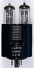
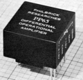
1953: A commercially available op amp. In 1953, vacuum tube op amps became commercially available with the release of the model K2-W from George A. Philbrick Researches, Incorporated. The designation on the devices shown, GAP/R, is an acronym for the complete company name. Two nine-pin 12AX7 vacuum tubes were mounted in an octal package and had a model K2-P chopper add-on available that would effectively "use up" the non-inverting input. This op amp was based on a descendant of Loebe Julie's 1947 design and, along with its successors, would start the widespread use of op amps in industry.
1961: A discrete IC op amp. With the birth of the transistor in 1947, and the silicon transistor in 1954, the concept of ICs became a reality. The introduction of the planar process in 1959 made transistors and ICs stable enough to be commercially useful. By 1961, solid-state, discrete op amps were being produced. These op amps were effectively small circuit boards with packages such as edge connectors. They usually had hand-selected resistors in order to improve things such as voltage offset and drift. The P45 (1961) had a gain of 94 dB and ran on ±15 V rails. It was intended to deal with signals in the range of ±10 V.
1961: A varactor bridge op amp. There have been many different directions taken in op-amp design. Varactor bridge op amps started to be produced in the early 1960s. They were designed to have extremely small input current and are still amongst the best op amps available in terms of common-mode rejection with the ability to correctly deal with hundreds of volts at their inputs.
1962: An op amp in a potted module. By 1962, several companies were producing modular potted packages that could be plugged into printed circuit boards. These packages were crucially important as they made the operational amplifier into a single black box which could be easily treated as a component in a larger circuit.
1963: A monolithic IC op amp. In 1963, the first monolithic IC op amp, the μA702 designed by Bob Widlar at Fairchild Semiconductor, was released. Monolithic ICs consist of a single chip as opposed to a chip and discrete parts (a discrete IC) or multiple chips bonded and connected on a circuit board (a hybrid IC). Almost all modern op amps are monolithic ICs; however, this first IC did not meet with much success. Issues such as an uneven supply voltage, low gain and a small dynamic range held off the dominance of monolithic op amps until 1965 when the μA709 (also designed by Bob Widlar) was released.
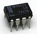
1968: Release of the μA741. The popularity of monolithic op amps was further improved upon the release of the LM101 in 1967, which solved a variety of issues, and the subsequent release of the μA741 in 1968. The μA741 was extremely similar to the LM101 except that Fairchild's facilities allowed them to include a 30 pF compensation capacitor inside the chip instead of requiring external compensation. This simple difference has made the 741 the canonical op amp and many modern amps base their pinout on the 741s. The μA741 is still in production, and has become ubiquitous in electronics—many manufacturers produce a version of this classic chip, recognizable by part numbers containing 741. The same part is manufactured by several companies.
1970: First high-speed, low-input current FET design. In the 1970s high speed, low-input current designs started to be made by using FETs. These would be largely replaced by op amps made with MOSFETs in the 1980s.
1972: Single sided supply op amps being produced. A single sided supply op amp is one where the input and output voltages can be as low as the negative power supply voltage instead of needing to be at least two volts above it. The result is that it can operate in many applications with the negative supply pin on the op amp being connected to the signal ground, thus eliminating the need for a separate negative power supply.
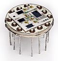
The LM324 (released in 1972) was one such op amp that came in a quad package (four separate op amps in one package) and became an industry standard. In addition to packaging multiple op amps in a single package, the 1970s also saw the birth of op amps in hybrid packages. These op amps were generally improved versions of existing monolithic op amps. As the properties of monolithic op amps improved, the more complex hybrid ICs were quickly relegated to systems that are required to have extremely long service lives or other specialty systems.
Recent trends. Recently supply voltages in analog circuits have decreased (as they have in digital logic) and low-voltage op amps have been introduced reflecting this. Supplies of 5 V and increasingly 3.3 V (sometimes as low as 1.8 V) are common. To maximize the signal range modern op amps commonly have rail-to-rail output (the output signal can range from the lowest supply voltage to the highest) and sometimes rail-to-rail inputs.
See also
In Spanish: Amplificador operacional para niños
- Active filter
- Analog computer
- Bob Widlar
- Current conveyor
- Current-feedback operational amplifier
- Differential amplifier
- George A. Philbrick
- Instrumentation amplifier
- Negative feedback amplifier
- Op-amp swapping
- Operational amplifier applications
- Operational transconductance amplifier
- Sallen–Key topology