Self-aligned gate facts for kids
A self-aligned gate is a clever way to build tiny electronic switches called transistors, which are found in almost all modern computers and phones. Imagine you're building a tiny LEGO structure. With self-aligned gates, the main part of the switch (the "gate") helps perfectly place the other parts (the "source" and "drain"). This makes the transistors smaller, faster, and more efficient.
This invention was a huge step forward in the 1970s and helped make computers much more powerful. Today, most integrated circuits (ICs, or "chips") still use this method.
Contents
How Chips Are Made
Building Tiny Switches
Computer chips are made in many steps on a thin, round slice of silicon called a "wafer". Think of it like building a layered cake. Each layer is created by covering the wafer with a special liquid called photoresist. Then, ultraviolet light shines through a stencil-like "mask" onto the photoresist.
The light changes the photoresist, making some parts hard and others soft. The soft parts are then washed away, leaving a tiny pattern on the wafer. The exposed parts of the silicon can then be changed. For example, the wafer might be heated to about 1000 degrees Celsius and exposed to a special gas. This gas adds "doping material" (like boron or phosphorus) to the silicon. This changes how electricity flows through the silicon, making it act like a conductor or an insulator. This is how the tiny transistors are formed.
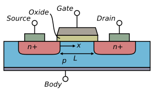
A MOSFET (Metal-Oxide-Semiconductor Field-Effect Transistor) has three main parts: the source, the drain, and the gate. When you apply a voltage to the gate, it creates an electric field. This field can turn the transistor "on" by allowing electricity to flow between the source and the drain. Because very little electricity flows through the gate itself, MOSFETs use very little power to switch on and off.
Older Ways of Building Transistors
In the past, the gate of a MOSFET was often made of aluminum. Aluminum melts at a much lower temperature (660 degrees Celsius) than the silicon is heated to during the doping process (around 1000 degrees Celsius). This meant the aluminum gate had to be added almost last, after all the high-temperature steps were done.
Here's how the old method worked:
- First, the source and drain areas were created by doping the silicon.
- Then, a thin layer of insulating material (silicon dioxide) was grown over the wafer.
- Finally, the aluminum gate was placed on top of the insulator using another mask.
To make sure the gate always connected properly with the source and drain, it had to be made much wider than the gap between them. This wasted space on the chip and created extra "parasitic capacitance." This extra capacitance meant the chip needed more power to work correctly, and it also made the chips slower. Plus, because the gate wasn't perfectly aligned every time, there were differences in how well each chip worked.
The Self-Aligned Solution
The idea of the self-aligned gate changed everything. Scientists discovered that heavily doped polysilicon (a type of silicon) could conduct electricity well enough to replace aluminum. This was a big deal because polysilicon can handle the high temperatures needed for doping.
With the self-aligned process:
- The insulating layer and the polysilicon gate are created early in the process.
- Then, the gate itself acts as a mask! When the source and drain areas are doped, the gate blocks the doping material from reaching the area directly underneath it.
- This means the source and drain are automatically lined up perfectly with the gate.
Because they are always perfectly aligned, the gate doesn't need to be made extra wide. This greatly reduces the wasted space and the parasitic capacitance. The chips become faster, use less power, and are more consistent from one chip to another.
This "silicon-gate technology" (SGT) also had other benefits. It allowed the transistor to be completely covered by a high-quality insulator, which led to new types of devices. For example, it made charge-coupled devices (CCDs) possible, which are used in digital cameras, and special memory devices that can store information even when the power is off.
To make self-aligned gates work, several new things were needed:
- New ways to create the gates.
- A change from a less stable form of silicon to polysilicon.
- New ways to etch (remove parts of) the polysilicon.
- Methods to make the silicon very pure.
History of Self-Aligned Gates
In 1966, a scientist named Robert W. Bower had the idea that if the gate was made first, it could help line up the other parts. He suggested using the aluminum gate as a mask. However, his method didn't work well in practice because aluminum couldn't handle the high temperatures needed for other steps.
In 1967, other researchers tried using a different type of silicon for the gate, but their method was only good for single transistors, not for complex chips.
Developing Silicon-Gate Technology
In 1968, a scientist at Fairchild Semiconductor named Tom Klein realized that using a specific type of doped silicon for the gate could lower the voltage needed to turn the transistor on. This was important for making faster and more power-efficient chips.
In February 1968, Federico Faggin joined Fairchild and took charge of developing this new low-voltage, self-aligned gate process. He figured out how to precisely etch the silicon gate and created all the detailed steps for making chips with silicon gates. He also invented "buried contacts," which allowed parts of the chip to connect directly without needing metal, making the chips even smaller.
By April 1968, Faggin had made the first working silicon-gate transistors. He then designed the first integrated circuit using this new technology, called the Fairchild 3708. This chip was much better than older ones: it was 5 times faster, used 100 times less power, and worked more reliably.
During this time, Faggin also made two other important improvements:
- He switched from evaporated silicon to polysilicon made by a different method, because the evaporated silicon would sometimes break over bumps on the chip.
- He used a process called "phosphorus gettering" to remove impurities from the transistors. This greatly improved their reliability.
Making it Commercial at Intel
The silicon-gate technology was adopted by Intel when the company started in 1968. Within a few years, it became the main way to make computer chips all over the world, and it's still used today. Intel also used this technology to create new types of memory that could store data even without power.
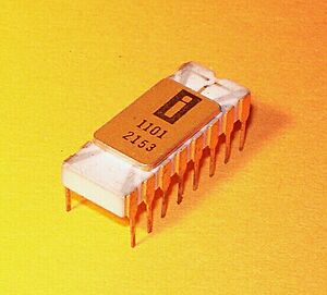
The first memory chip to use silicon-gate technology was the Intel 1101 SRAM chip, made in 1968. The first commercial single-chip microprocessor, the Intel 4004, was also developed by Federico Faggin using his silicon-gate MOS IC technology.
How Self-Aligned Gates Are Made
The process of making self-aligned gates is important because it simplifies how chips are built and makes them much more reliable.
Here are the main steps:
- 1. First, small areas are etched into the silicon wafer where the transistors will be. Each area defines where the source, drain, and gate will be.
- 2. A very thin layer of insulating material, called gate oxide, is grown on the silicon wafer.
- 3. A layer of polysilicon is added on top of the gate oxide.
- 4. A special liquid called photoresist is put on top of the polysilicon.
- 5. A mask is placed over the photoresist, and UV light shines through it. This light breaks down the photoresist in the areas not covered by the mask.
- 6. A special liquid washes away the photoresist that was broken down by the UV light.
- 7. The polysilicon and gate oxide that are not covered by the remaining photoresist are etched away. This leaves the polysilicon gate in place.
- 8. The rest of the photoresist is removed. Now, you have a wafer with the polysilicon gate sitting on top of the gate oxide.
- 9. The thin oxide layer is etched away from the source and drain regions, but the gate area is protected by the polysilicon gate.
- 10. Now, the source, drain, and polysilicon gate are "doped" with special materials. The polysilicon gate acts as a mask, making sure the source and drain areas are perfectly lined up with it. This is the "self-aligning" step!
- 11. The wafer is heated in a furnace. This helps the doping materials spread deeper into the silicon, forming the final source and drain regions.
- 12. Finally, more layers are added to protect the chip and connect all the parts, completing the process.
See also


