Leo Esaki facts for kids
Quick facts for kids
Leo Esaki
|
|
|---|---|
| 江崎 玲於奈 | |

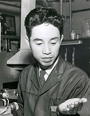
Esaki in 1959
|
|
| Born | March 12, 1925 Takaida-mura, Nakakawachi-gun, Osaka Prefecture, Imperial Japan
|
| Alma mater | Tokyo Imperial University (BSc, PhD) |
| Known for |
|
| Title | IBM Fellow (1967–1992) |
| Awards |
|
| Honors |
|
| Scientific career | |
| Fields | Solid-state physics |
| Institutions |
|
Leo Esaki (born March 12, 1925) is a Japanese scientist who studies how materials behave. He is known for his work on something called quantum tunneling in materials called semiconductors. This research led him to invent the tunnel diode. In 1973, he shared the Nobel Prize in Physics for these important discoveries. He also helped create a new idea called superlattices.
Contents
Early Life and School
Leo Esaki was born in a place called Takaida-mura in Japan. He grew up in Kyoto. He went to Doshisha Junior High School and then the Third Higher School. After that, he studied physics at the University of Tokyo. He was at the university during the Bombing of Tokyo in World War II.
He earned his first degree in 1947 and his PhD in 1959, both from the University of Tokyo.
Amazing Discoveries and Career
The Esaki Diode: A Tiny Breakthrough
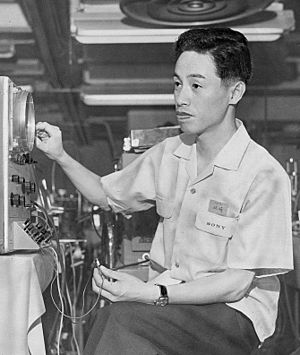
From 1947 to 1960, Esaki worked at companies that later became Denso Ten and Sony. Around this time, other scientists invented the transistor. This made Esaki interested in studying special materials like germanium and silicon.
He found something amazing: if he made a part of these materials very, very thin, electricity could pass through it in a strange way. This was due to something called the tunnel effect. He noticed that as he increased the voltage, the electric current would actually decrease. This is called negative resistance.
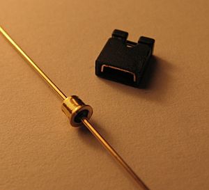
This discovery was the first time anyone had shown the tunnel effect in solid materials. It led to the invention of the Esaki diode, also known as the tunnel diode. This was the first quantum electronic device ever made! Because of this big invention, he received his doctorate degree in 1959.
In 1973, Esaki won the Nobel Prize for his work on electron tunneling. He was the first Nobel winner to receive the award from King Carl XVI Gustaf of Sweden.
Superlattices: Building New Materials
In 1960, Esaki moved to the United States and joined IBM's T. J. Watson Research Center. He became an important scientist there in 1967.
He had a new idea: what if you could build materials with many super-thin layers, one on top of the other? He called these semiconductor superlattices. He thought these layers could create new and useful properties. He developed a special way to grow these thin layers, almost like building with tiny atoms.
His first paper about superlattices came out in 1970. At first, some people thought his idea was "too speculative" and wouldn't work. But his research was later supported by the Army Research Office.
In 1972, Esaki successfully created these superlattices. His idea has since helped many areas of science, including metals and magnetic materials. He received the IEEE Medal of Honor in 1991 and the Japan Prize in 1998 for his work on creating these amazing new materials.
Esaki's "Five Don'ts" for Creativity
In 1994, Leo Esaki shared five rules he believes can help anyone be more creative. These rules are:
- Don't let your past experiences hold you back.
- Don't rely too much on just one expert in your field.
- Don't hold onto things you don't need anymore.
- Don't be afraid to face challenges.
- Always keep your childhood curiosity alive.
Later Years and Recognition
Esaki moved back to Japan in 1992. He became the president of the University of Tsukuba and later the Shibaura Institute of Technology. Since 2006, he has been the president of Yokohama College of Pharmacy.
He has received many awards, including the Order of Culture in 1974 and the Grand Cordon of the Order of the Rising Sun in 1998.
After another Japanese Nobel winner, Yoichiro Nambu, passed away in 2015, Esaki became the oldest living Japanese Nobel laureate.
In 2015, bronze statues of three Nobel winners, including Leo Esaki, were placed in Central Park in Tsukuba City to honor their contributions.
Awards and Honors
- 1959 – Asahi Prize
- 1959 – Nishina Memorial Prize
- 1961 – Stuart Ballantine Medal
- 1965 – Japan Academy Prize
- 1973 – Nobel Prize in Physics
- 1974 – Order of Culture
- 1985 – James C. McGroddy Prize for New Materials
- 1989 – Harold Pender Award
- 1991 – IEEE Medal of Honor
- 1998 – Japan Prize
- 1998 – Grand Cordon of the Order of the Rising Sun
- 2001 – Honorary Doctor at the Hong Kong University of Science and Technology
- 2007 – Honorary Distinguished Professor at the National Tsing Hua University
Memberships in Science Groups
- 1960 Fellow of the American Physical Society
- Physical Society of Japan
- 1975 – Member, the Japan Academy
- 1976 – Foreign Associate, National Academy of Sciences
- 1977 – Foreign Associate, National Academy of Engineering
- 1989 – Member, Max Planck Society
- 1991 – Member, American Philosophical Society
- 1994 – Foreign Member, Russian Academy of Sciences
- 1995 – Honorary Foreign Member, Korean Academy of Science and Technology
- 1996 – Member, Accademia dei Lincei
See also
 In Spanish: Leo Esaki para niños
- List of Japanese Nobel laureates
- List of Nobel laureates affiliated with the University of Tokyo


