Czochralski method facts for kids
The Czochralski method, also called the Czochralski technique or Czochralski process, is a way to grow very pure single crystals. It's used to make crystals of materials like semiconductors (such as silicon and germanium), metals (like palladium and gold), salts, and even fake gemstones.
This method is named after a Polish scientist named Jan Czochralski. He invented it by accident in 1915 while studying how fast metals crystallize. Instead of dipping his pen into his inkwell, he dipped it into melted tin. When he pulled his pen out, it had a long, thin piece of tin attached, which turned out to be a single crystal! Today, this method is still used for over 90 percent of all electronics that use semiconductors.
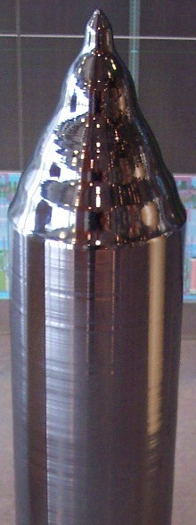
One of the most important uses of the Czochralski method is growing large, cylinder-shaped pieces, called boules, of single crystal silicon. These are essential for the electronics industry to create semiconductor devices like integrated circuits (the tiny "brains" in computers and phones). Other semiconductors, like gallium arsenide, can also be grown this way. The method can even make super-pure salt crystals for science experiments, like those in particle physics.
Contents
What is Czochralski Silicon Used For?
Monocrystalline silicon (often called mono-Si) made using the Czochralski method is known as monocrystalline Czochralski silicon (Cz-Si). This special silicon is the main material for making integrated circuits. These circuits are found in almost all electronic devices, from computers and TVs to mobile phones.
Mono-Si is also used a lot in the photovoltaic industry. This means it's used to make regular mono-Si solar cells. Because its crystal structure is almost perfect, it's very good at turning sunlight into electricity. This gives silicon solar cells their best possible efficiency.
How Czochralski Silicon is Made
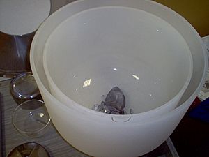
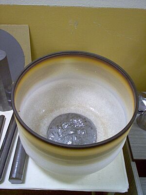
First, very pure silicon, which has only tiny amounts of impurities, is melted in a special container called a crucible. This container is usually made of quartz. The silicon melts at about 1,425 °C (2,597 °F; 1,698 K).
Sometimes, small amounts of other atoms, called dopants, are added to the melted silicon. These can be atoms like boron or phosphorus. Adding dopants changes the silicon's electrical properties, making it either p-type or n-type.
Next, a small, perfectly shaped seed crystal on a rod is dipped into the melted silicon. The rod holding the seed crystal is then slowly pulled upwards and rotated at the same time. By carefully controlling the temperature, how fast it's pulled, and how fast it spins, a large, single-crystal cylinder, called an ingot, can be pulled out of the melt. This whole process usually happens in a sealed chamber filled with a gas like argon, which doesn't react with the silicon.
How Big Can These Crystals Get?
To make things more efficient, the electronics industry uses silicon slices, called wafers, that are standard sizes. In the past, the crystal boules were small, only a few centimeters wide. But with new technology, manufacturers now use wafers that are 200 mm (about 8 inches) and even 300 mm (about 12 inches) across!
The width of the crystal is controlled very precisely. This is done by adjusting the temperature, the rotation speeds, and how fast the seed crystal is pulled up. The crystal ingots that these wafers are sliced from can be up to 2 meters (about 6.5 feet) long and weigh hundreds of kilograms!
Larger wafers are better for manufacturing because more chips can be made on each one. This means less waste and lower costs. So, there's always a push to make silicon wafers even bigger. The next size, 450 mm, was planned for the future. Silicon wafers are usually quite thin, about 0.2 to 0.75 mm thick. They can be polished very flat for making integrated circuits or given a texture for making solar cells.
What About Impurities?
When silicon is grown using the Czochralski method, the melted silicon is held in a silica (or quartz) crucible. As the crystal grows, tiny bits of the crucible walls dissolve into the melted silicon. Because of this, Czochralski silicon usually contains some oxygen.
This oxygen can be helpful or harmful. If handled carefully, the oxygen can form tiny clumps inside the silicon. These clumps can trap unwanted metal impurities, making the surrounding silicon even purer. This process is called gettering. However, if oxygen clumps form in the wrong places, they can damage the electrical parts of a device.
Oxygen can also make silicon wafers stronger. It helps to fix any tiny flaws that might appear during the manufacturing process. Scientists also found in the 1990s that a lot of oxygen in silicon helps it resist damage from radiation. This is important for things like particle detectors used in big science experiments, such as those at CERN's LHC.
However, oxygen in silicon can also cause problems for solar cells. When sunlight hits a solar cell, the oxygen can react with boron (another impurity) to form something that makes the cell less efficient. This can cause the solar cell's power output to drop a little during its first few hours of light exposure.
See also
- Float-zone silicon


