kids encyclopedia robot

ARM architecture family facts for kids

Kids Encyclopedia Facts
Quick facts for kids
ARM
Arm logo 2017.svg
Designer
Bits 32-bit, 64-bit
Introduced 1985; 40 years ago (1985)
Design RISC
Type Register-Register
Branching Condition code, compare and branch
Open Proprietary
ARM 64/32-bit
Introduced 2011; 14 years ago (2011)
Version ARMv8-R, ARMv8-A, ARMv8.1-A, ARMv8.2-A, ARMv8.3-A, ARMv8.4-A, ARMv8.5-A, ARMv8.6-A, ARMv8.7-A, ARMv8.8-A, ARMv8.9-A, ARMv9.0-A, ARMv9.1-A, ARMv9.2-A, ARMv9.3-A, ARMv9.4-A
Encoding AArch64/A64 and AArch32/A32 use 32-bit instructions, T32 (Thumb-2) uses mixed 16- and 32-bit instructions
Endianness Bi (little as default)
Extensions SVE, SVE2, SME, AES, SHA, TME; All mandatory: Thumb-2, Neon, VFPv4-D16, VFPv4; obsolete: Jazelle
Registers
General purpose 31 × 64-bit integer registers
Floating point 32 × 128-bit registers for scalar 32- and 64-bit FP or SIMD FP or integer; or cryptography
ARM 32-bit (Cortex)
Version ARMv9-R, ARMv9-M, ARMv8-R, ARMv8-M, ARMv7-A, ARMv7-R, ARMv7E-M, ARMv7-M, ARMv6-M
Encoding 32-bit, except Thumb-2 extensions use mixed 16- and 32-bit instructions.
Endianness Bi (little as default)
Extensions Thumb-2, Neon, Jazelle, AES, SHA, DSP, Saturated, FPv4-SP, FPv5, Helium
Registers
General purpose 15 × 32-bit integer registers, including R14 (link register), but not R15 (PC)
Floating point Up to 32 × 64-bit registers, SIMD/floating-point (optional)
ARM 32-bit (legacy)
Version ARMv6, ARMv5, ARMv4T, ARMv3, ARMv2
Encoding 32-bit, except Thumb extension uses mixed 16- and 32-bit instructions.
Endianness Bi (little as default) in ARMv3 and above
Extensions Thumb, Jazelle
Registers
General purpose 15 × 32-bit integer registers, including R14 (link register), but not R15 (PC, 26-bit addressing in older)
Floating point None

ARM (stylised in lowercase as arm, formerly an acronym for Advanced RISC Machines and originally Acorn RISC Machine) is a family of RISC instruction set architectures for computer processors, configured for various environments. Arm Ltd. develops the architectures and licenses them to other companies, who design their own products that implement one or more of those architectures, including system on a chip (SoC) and system on module (SOM) designs, that incorporate different components such as memory, interfaces, and radios. It also designs cores that implement these instruction set architectures and licenses these designs to many companies that incorporate those core designs into their own products.

Due to their low costs, minimal power consumption, and lower heat generation than their competitors, ARM processors are desirable for light, portable, battery-powered devices, including smartphones, laptops and tablet computers, and other embedded systems. However, ARM processors are also used for desktops and servers, including the world's fastest supercomputer (Fugaku) from 2020 to 2022. With over 230 billion ARM chips produced, as of 2022, ARM is the most widely used family of instruction set architectures (ISA) and the ISAs produced in the largest quantity. Currently, the widely used Cortex cores, older "classic" cores, and specialised SecurCore cores variants are available for each of these to include or exclude optional capabilities.

There have been several generations of the ARM design. The original ARM1 used a 32-bit internal structure but had a 26-bit address space that limited it to 64 MB of main memory. This limitation was removed in the ARMv3 series, which has a 32-bit address space, and several additional generations up to ARMv7 remained 32-bit. Released in 2011, the ARMv8-A architecture added support for a 64-bit address space and 64-bit arithmetic with its new 32-bit fixed-length instruction set. Arm Ltd. has also released a series of additional instruction sets for different rules; the "Thumb" extension adds both 32- and 16-bit instructions for improved code density, while Jazelle added instructions for directly handling Java bytecode. More recent changes include the addition of simultaneous multithreading (SMT) for improved performance or fault tolerance.

History

BBC Micro

Acorn Computers' first widely successful design was the BBC Micro, introduced in December 1981. This was a relatively conventional machine based on the MOS Technology 6502 CPU but ran at roughly double the performance of competing designs like the Apple II due to its use of faster dynamic random-access memory (DRAM). Typical DRAM of the era ran at about 2 MHz; Acorn arranged a deal with Hitachi for a supply of faster 4 MHz parts.

Machines of the era generally shared memory between the processor and the framebuffer, which allowed the processor to quickly update the contents of the screen without having to perform separate input/output (I/O). As the timing of the video display is exacting, the video hardware had to have priority access to that memory. Due to a quirk of the 6502's design, the CPU left the memory untouched for half of the time. Thus by running the CPU at 1 MHz, the video system could read data during those down times, taking up the total 2 MHz bandwidth of the RAM. In the BBC Micro, the use of 4 MHz RAM allowed the same technique to be used, but running at twice the speed. This allowed it to outperform any similar machine on the market.

Acorn Business Computer

1981 was also the year that the IBM Personal Computer was introduced. Using the recently introduced Intel 8088, a 16-bit CPU compared to the 6502's 8-bit design, it offered higher overall performance. Its introduction changed the desktop computer market radically: what had been largely a hobby and gaming market emerging over the prior five years began to change to a must-have business tool where the earlier 8-bit designs simply could not compete. Even newer 32-bit designs were also coming to market, such as the Motorola 68000 and National Semiconductor NS32016.

Acorn began considering how to compete in this market and produced a new paper design named the Acorn Business Computer. They set themselves the goal of producing a machine with ten times the performance of the BBC Micro, but at the same price. This would outperform and underprice the PC. At the same time, the recent introduction of the Apple Lisa brought the graphical user interface (GUI) concept to a wider audience and suggested the future belonged to machines with a GUI. The Lisa, however, cost $9,995, as it was packed with support chips, large amounts of memory, and a hard disk drive, all very expensive then.

The engineers then began studying all of the CPU designs available. Their conclusion about the existing 16-bit designs was that they were a lot more expensive, offering only slightly higher performance than their BBC Micro design. They also almost always demanded a large number of support chips to operate even at that level, which drove up the cost of the computer as a whole. These systems would simply not hit the design goal. They also considered the new 32-bit designs, but these cost even more and had the same issues with support chips. According to Sophie Wilson, all the processors tested at that time performed about the same, with about a 4 Mbit/second bandwidth.

Two key events led Acorn down the path to ARM. One was the publication of a series of reports from the University of California, Berkeley, which suggested that a simple chip design could nevertheless have extremely high performance, much higher than the latest 32-bit designs on the market. The second was a visit by Steve Furber and Sophie Wilson to the Western Design Center, a company run by Bill Mensch and his sister, which had become the logical successor to the MOS team and was offering new versions like the WDC 65C02. The Acorn team saw high school students producing chip layouts on Apple II machines, which suggested that anyone could do it. In contrast, a visit to another design firm working on modern 32-bit CPU revealed a team with over a dozen members which were already on revision H of their design and yet it still contained bugs. This cemented their late 1983 decision to begin their own CPU design, the Acorn RISC Machine.

Design concepts

The original Berkeley RISC designs were in some sense teaching systems, not designed specifically for outright performance. To the RISC's basic register-heavy and load/store concepts, ARM added a number of the well-received design notes of the 6502. Primary among them was the ability to quickly serve interrupts, which allowed the machines to offer reasonable input/output performance with no added external hardware. To offer interrupts with similar performance as the 6502, the ARM design limited its physical address space to 64 MB of total addressable space, requiring 26 bits of address. As instructions were 4 bytes (32 bits) long, and required to be aligned on 4-byte boundaries, the lower 2 bits of an instruction address were always zero. This meant the program counter (PC) only needed to be 24 bits, allowing it to be stored along with the eight bit processor flags in a single 32-bit register. That meant that upon receiving an interrupt, the entire machine state could be saved in a single operation, whereas had the PC been a full 32-bit value, it would require separate operations to store the PC and the status flags. This decision halved the interrupt overhead.

Another change, and among the most important in terms of practical real-world performance, was the modification of the instruction set to take advantage of page mode DRAM. Recently introduced, page mode allowed subsequent accesses of memory to run twice as fast if they were roughly in the same location, or "page", in the DRAM chip. Berkeley's design did not consider page mode and treated all memory equally. The ARM design added special vector-like memory access instructions, the "S-cycles", that could be used to fill or save multiple registers in a single page using page mode. This doubled memory performance when they could be used, and was especially important for graphics performance.

The Berkeley RISC designs used register windows to reduce the number of register saves and restores performed in procedure calls; the ARM design did not adopt this.

Wilson developed the instruction set, writing a simulation of the processor in BBC BASIC that ran on a BBC Micro with a second 6502 processor. This convinced Acorn engineers they were on the right track. Wilson approached Acorn's CEO, Hermann Hauser, and requested more resources. Hauser gave his approval and assembled a small team to design the actual processor based on Wilson's ISA. The official Acorn RISC Machine project started in October 1983.

ARM1

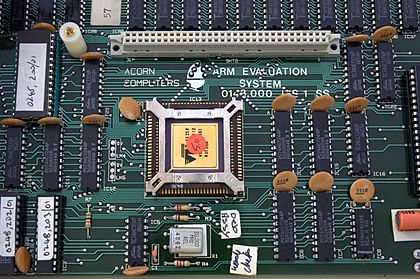
Acorn-ARM-Evaluation-System
ARM1 2nd processor for the BBC Micro

Acorn chose VLSI Technology as the "silicon partner", as they were a source of ROMs and custom chips for Acorn. Acorn provided the design and VLSI provided the layout and production. The first samples of ARM silicon worked properly when first received and tested on 26 April 1985. Known as ARM1, these versions ran at 6 MHz.

The first ARM application was as a second processor for the BBC Micro, where it helped in developing simulation software to finish development of the support chips (VIDC, IOC, MEMC), and sped up the CAD software used in ARM2 development. Wilson subsequently rewrote BBC BASIC in ARM assembly language. The in-depth knowledge gained from designing the instruction set enabled the code to be very dense, making ARM BBC BASIC an extremely good test for any ARM emulator.

ARM2

The result of the simulations on the ARM1 boards led to the late 1986 introduction of the ARM2 design running at 8 MHz, and the early 1987 speed-bumped version at 10 to 12 MHz. A significant change in the underlying architecture was the addition of a Booth multiplier, whereas formerly multiplication had to be carried out in software. Further, a new Fast Interrupt reQuest mode, FIQ for short, allowed registers 8 through 14 to be replaced as part of the interrupt itself. This meant FIQ requests did not have to save out their registers, further speeding interrupts.

The ARM2 was roughly seven times the performance of a typical 7 MHz 68000-based system like the Amiga or Macintosh SE. It was twice as fast as an Intel 80386 running at 16 MHz, and about the same speed as a multi-processor VAX-11/784 superminicomputer. The only systems that beat it were the Sun SPARC and MIPS R2000 RISC-based workstations. Further, as the CPU was designed for high-speed I/O, it dispensed with many of the support chips seen in these machines; notably, it lacked any dedicated direct memory access (DMA) controller which was often found on workstations. The graphics system was also simplified based on the same set of underlying assumptions about memory and timing. The result was a dramatically simplified design, offering performance on par with expensive workstations but at a price point similar to contemporary desktops.

The ARM2 featured a 32-bit data bus, 26-bit address space and 27 32-bit registers, of which 16 are accessible at any one time (including the PC). The ARM2 had a transistor count of just 30,000, compared to Motorola's six-year-older 68000 model with around 68,000. Much of this simplicity came from the lack of microcode, which represents about one-quarter to one-third of the 68000's transistors, and the lack of (like most CPUs of the day) a cache. This simplicity enabled the ARM2 to have a low power consumption and simpler thermal packaging, through having fewer powered transistors, yet offering better performance than the contemporary, 1987, IBM PS/2 Model 50, which initially utilised an Intel 80286, offering 1.8 MIPS @ 10 MHz, and later in 1987, the 2 MIPS of the PS/2 70, with its Intel 386 DX @ 16 MHz.

A successor, ARM3, was produced with a 4 KB cache, which further improved performance. The address bus was extended to 32 bits in the ARM6, but program code still had to lie within the first 64 MB of memory in 26-bit compatibility mode, due to the reserved bits for the status flags.

Advanced RISC Machines Ltd. – ARM6

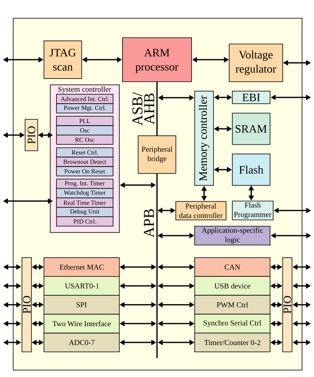
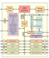
ARMSoCBlockDiagram
Microprocessor-based system on a chip
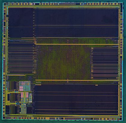
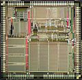
GPS ARM610 die
Die of an ARM610 microprocessor

In the late 1980s, Apple Computer and VLSI Technology started working with Acorn on newer versions of the ARM core. In 1990, Acorn spun off the design team into a new company named Advanced RISC Machines Ltd., which became ARM Ltd. when its parent company, Arm Holdings plc, floated on the London Stock Exchange and Nasdaq in 1998. The new Apple–ARM work would eventually evolve into the ARM6, first released in early 1992. Apple used the ARM6-based ARM610 as the basis for their Apple Newton PDA.

Early licensees

In 1994, Acorn used the ARM610 as the main central processing unit (CPU) in their RiscPC computers. DEC licensed the ARMv4 architecture and produced the StrongARM. At 233 MHz, this CPU drew only one watt (newer versions draw far less). This work was later passed to Intel as part of a lawsuit settlement, and Intel took the opportunity to supplement their i960 line with the StrongARM. Intel later developed its own high performance implementation named XScale, which it has since sold to Marvell. Transistor count of the ARM core remained essentially the same throughout these changes; ARM2 had 30,000 transistors, while ARM6 grew only to 35,000.

Market share

In 2005, about 98% of all mobile phones sold used at least one ARM processor. In 2010, producers of chips based on ARM architectures reported shipments of 6.1 billion ARM-based processors, representing 95% of smartphones, 35% of digital televisions and set-top boxes, and 10% of mobile computers. In 2011, the 32-bit ARM architecture was the most widely used architecture in mobile devices and the most popular 32-bit one in embedded systems. In 2013, 10 billion were produced and "ARM-based chips are found in nearly 60 percent of the world's mobile devices".

Licensing

STM32F103VGT6-HD
Die of a STM32F103VGT6 ARM Cortex-M3 microcontroller with 1 MB flash memory by STMicroelectronics

Core licence

Arm Ltd.'s primary business is selling IP cores, which licensees use to create microcontrollers (MCUs), CPUs, and systems-on-chips based on those cores. The original design manufacturer combines the ARM core with other parts to produce a complete device, typically one that can be built in existing semiconductor fabrication plants (fabs) at low cost and still deliver substantial performance. The most successful implementation has been the ARM7TDMI with hundreds of millions sold. Atmel has been a precursor design center in the ARM7TDMI-based embedded system.

The ARM architectures used in smartphones, PDAs and other mobile devices range from ARMv5 to ARMv8-A.

In 2009, some manufacturers introduced netbooks based on ARM architecture CPUs, in direct competition with netbooks based on Intel Atom.

Arm Ltd. offers a variety of licensing terms, varying in cost and deliverables. Arm Ltd. provides to all licensees an integratable hardware description of the ARM core as well as complete software development toolset (compiler, debugger, software development kit), and the right to sell manufactured silicon containing the ARM CPU.

SoC packages integrating ARM's core designs include Nvidia Tegra's first three generations, CSR plc's Quatro family, ST-Ericsson's Nova and NovaThor, Silicon Labs's Precision32 MCU, Texas Instruments's OMAP products, Samsung's Hummingbird and Exynos products, Apple's A4, A5, and A5X, and NXP's i.MX.

Fabless licensees, who wish to integrate an ARM core into their own chip design, are usually only interested in acquiring a ready-to-manufacture verified semiconductor intellectual property core. For these customers, Arm Ltd. delivers a gate netlist description of the chosen ARM core, along with an abstracted simulation model and test programs to aid design integration and verification. More ambitious customers, including integrated device manufacturers (IDM) and foundry operators, choose to acquire the processor IP in synthesizable RTL (Verilog) form. With the synthesizable RTL, the customer has the ability to perform architectural level optimisations and extensions. This allows the designer to achieve exotic design goals not otherwise possible with an unmodified netlist (high clock speed, very low power consumption, instruction set extensions, etc.). While Arm Ltd. does not grant the licensee the right to resell the ARM architecture itself, licensees may freely sell manufactured products such as chip devices, evaluation boards and complete systems. Merchant foundries can be a special case; not only are they allowed to sell finished silicon containing ARM cores, they generally hold the right to re-manufacture ARM cores for other customers.

Arm Ltd. prices its IP based on perceived value. Lower performing ARM cores typically have lower licence costs than higher performing cores. In implementation terms, a synthesisable core costs more than a hard macro (blackbox) core. Complicating price matters, a merchant foundry that holds an ARM licence, such as Samsung or Fujitsu, can offer fab customers reduced licensing costs. In exchange for acquiring the ARM core through the foundry's in-house design services, the customer can reduce or eliminate payment of ARM's upfront licence fee.

Compared to dedicated semiconductor foundries (such as TSMC and UMC) without in-house design services, Fujitsu/Samsung charge two- to three-times more per manufactured wafer. For low to mid volume applications, a design service foundry offers lower overall pricing (through subsidisation of the licence fee). For high volume mass-produced parts, the long term cost reduction achievable through lower wafer pricing reduces the impact of ARM's NRE (non-recurring engineering) costs, making the dedicated foundry a better choice.

Companies that have developed chips with cores designed by Arm include Amazon.com's Annapurna Labs subsidiary, Analog Devices, Apple, AppliedMicro (now: MACOM Technology Solutions), Atmel, Broadcom, Cavium, Cypress Semiconductor, Freescale Semiconductor (now NXP Semiconductors), Huawei, Intel, Maxim Integrated, Nvidia, NXP, Qualcomm, Renesas, Samsung Electronics, ST Microelectronics, Texas Instruments, and Xilinx.

Built on ARM Cortex Technology licence

In February 2016, ARM announced the Built on ARM Cortex Technology licence, often shortened to Built on Cortex (BoC) licence. This licence allows companies to partner with ARM and make modifications to ARM Cortex designs. These design modifications will not be shared with other companies. These semi-custom core designs also have brand freedom, for example Kryo 280.

Companies that are current licensees of Built on ARM Cortex Technology include Qualcomm.

Architectural licence

Companies can also obtain an ARM architectural licence for designing their own CPU cores using the ARM instruction sets. These cores must comply fully with the ARM architecture. Companies that have designed cores that implement an ARM architecture include Apple, AppliedMicro (now: Ampere Computing), Broadcom, Cavium (now: Marvell), Digital Equipment Corporation, Intel, Nvidia, Qualcomm, Samsung Electronics, Fujitsu, and NUVIA Inc. (acquired by Qualcomm in 2021).

ARM Flexible Access

On 16 July 2019, ARM announced ARM Flexible Access. ARM Flexible Access provides unlimited access to included ARM intellectual property (IP) for development. Per product licence fees are required once a customer reaches foundry tapeout or prototyping.

75% of ARM's most recent IP over the last two years are included in ARM Flexible Access. As of October 2019:

  • CPUs: Cortex-A5, Cortex-A7, Cortex-A32, Cortex-A34, Cortex-A35, Cortex-A53, Cortex-R5, Cortex-R8, Cortex-R52, Cortex-M0, Cortex-M0+, Cortex-M3, Cortex-M4, Cortex-M7, Cortex-M23, Cortex-M33
  • GPUs: Mali-G52, Mali-G31. Includes Mali Driver Development Kits (DDK).
  • Interconnect: CoreLink NIC-400, CoreLink NIC-450, CoreLink CCI-400, CoreLink CCI-500, CoreLink CCI-550, ADB-400 AMBA, XHB-400 AXI-AHB
  • System Controllers: CoreLink GIC-400, CoreLink GIC-500, PL192 VIC, BP141 TrustZone Memory Wrapper, CoreLink TZC-400, CoreLink L2C-310, CoreLink MMU-500, BP140 Memory Interface
  • Security IP: CryptoCell-312, CryptoCell-712, TrustZone True Random Number Generator
  • Peripheral Controllers: PL011 UART, PL022 SPI, PL031 RTC
  • Debug & Trace: CoreSight SoC-400, CoreSight SDC-600, CoreSight STM-500, CoreSight System Trace Macrocell, CoreSight Trace Memory Controller
  • Design Kits: Corstone-101, Corstone-201
  • Physical IP: Artisan PIK for Cortex-M33 TSMC 22ULL including memory compilers, logic libraries, GPIOs and documentation
  • Tools & Materials: Socrates IP ToolingARM Design Studio, Virtual System Models
  • Support: Standard ARM Technical support, ARM online training, maintenance updates, credits toward onsite training and design reviews

Cores

Architecture Core
bit-width
Cores Profile Refe-
rences
Arm Ltd. Third-party
ARMv1
32
ARM1
Classic
ARMv2
32
ARM2, ARM250, ARM3 Amber, STORM Open Soft Core
Classic
ARMv3
32
ARM6, ARM7
Classic
ARMv4
32
ARM8 StrongARM, FA526, ZAP Open Source Processor Core
Classic
ARMv4T
32
ARM7TDMI, ARM9TDMI, SecurCore SC100
Classic
ARMv5TE
32
ARM7EJ, ARM9E, ARM10E XScale, FA626TE, Feroceon, PJ1/Mohawk
Classic
ARMv6
32
ARM11
Classic
ARMv6-M
32
ARM Cortex-M0, ARM Cortex-M0+, ARM Cortex-M1, SecurCore SC000
Microcontroller
ARMv7-M
32
ARM Cortex-M3, SecurCore SC300 Apple M7 motion coprocessor
Microcontroller
ARMv7E-M
32
ARM Cortex-M4, ARM Cortex-M7
Microcontroller
ARMv8-M
32
ARM Cortex-M23, ARM Cortex-M33
Microcontroller
ARMv7-R
32
ARM Cortex-R4, ARM Cortex-R5, ARM Cortex-R7, ARM Cortex-R8
Real-time
ARMv8-R
32
ARM Cortex-R52
Real-time
64
ARM Cortex-R82
Real-time
ARMv7-A
32
ARM Cortex-A5, ARM Cortex-A7, ARM Cortex-A8, ARM Cortex-A9, ARM Cortex-A12, ARM Cortex-A15, ARM Cortex-A17 Qualcomm Scorpion/Krait, PJ4/Sheeva, Apple Swift (A6, A6X)
Application
ARMv8-A
32
ARM Cortex-A32
Application
64/32
ARM Cortex-A35, ARM Cortex-A53, ARM Cortex-A57, ARM Cortex-A72, ARM Cortex-A73 X-Gene, Nvidia Denver 1/2, Cavium ThunderX, AMD K12, Apple Cyclone (A7)/Typhoon (A8, A8X)/Twister (A9, A9X)/Hurricane+Zephyr (A10, A10X), Qualcomm Kryo, Samsung M1/M2 ("Mongoose") /M3 ("Meerkat")
Application
64
ARM Cortex-A34
Application
ARMv8.1-A
64/32
0TBA Cavium ThunderX2
Application
ARMv8.2-A
64/32
ARM Cortex-A55, ARM Cortex-A75, ARM Cortex-A76, ARM Cortex-A77, ARM Cortex-A78, ARM Cortex-X1, ARM Neoverse N1 Nvidia Carmel, Samsung M4 ("Cheetah"), Fujitsu A64FX (ARMv8 SVE 512-bit)
Application
64
ARM Cortex-A65, ARM Neoverse E1 with simultaneous multithreading (SMT), ARM Cortex-A65AE (also having e.g. ARMv8.4 Dot Product; made for safety critical tasks such as advanced driver-assistance systems (ADAS)) Apple Monsoon+Mistral (A11) (September 2017)
Application
ARMv8.3-A
64/32
0TBA
Application
64
0TBA Apple Vortex+Tempest (A12, A12X, A12Z), Marvell ThunderX3 (v8.3+)
Application
ARMv8.4-A
64/32
0TBA
Application
64
ARM Neoverse V1 Apple Lightning+Thunder (A13), Apple Firestorm+Icestorm (A14, M1)
Application
ARMv8.5-A
64/32
0TBA
Application
64
0TBA
Application
ARMv8.6-A
64
0TBA Apple Avalanche+Blizzard (A15, M2), Apple Everest+Sawtooth (A16)
Application
ARMv8.7-A
64
0TBA
Application
ARMv8.8-A
64
0TBA
Application
ARMv8.9-A
64
0TBA
Application
ARMv9.0-A
64
ARM Cortex-A510, ARM Cortex-A710, ARM Cortex-A715, ARM Cortex-X2, ARM Cortex-X3, ARM Neoverse E2, ARM Neoverse N2, ARM Neoverse V2
Application
ARMv9.1-A
64
0TBA
Application
ARMv9.2-A
64
ARM Cortex-A520, ARM Cortex-A720, ARM Cortex-X4 Qualcomm Snapdragon 8 Gen 3, Mediatek Dimensity 9300
Application
ARMv9.3-A
64
0TBA
Application
ARMv9.4-A
64
0TBA
Application

Arm provides a list of vendors who implement ARM cores in their design (application specific standard products (ASSP), microprocessor and microcontrollers).

Example applications of ARM cores

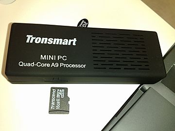
Quad-core Android "mini PC", with a microSD card next to it for a size comparison
Tronsmart MK908, a Rockchip-based quad-core Android "mini PC", with a microSD card next to it for a size comparison

ARM cores are used in a number of products, particularly PDAs and smartphones. Some computing examples are Microsoft's first generation Surface, Surface 2 and Pocket PC devices (following 2002), Apple's iPads, and Asus's Eee Pad Transformer tablet computers, and several Chromebook laptops. Others include Apple's iPhone smartphones and iPod portable media players, Canon PowerShot digital cameras, Nintendo Switch hybrid, the Wii security processor and 3DS handheld game consoles, and TomTom turn-by-turn navigation systems.

In 2005, Arm took part in the development of Manchester University's computer SpiNNaker, which used ARM cores to simulate the human brain.

ARM chips are also used in Raspberry Pi, BeagleBoard, BeagleBone, PandaBoard, and other single-board computers, because they are very small, inexpensive, and consume very little power.

32-bit architecture

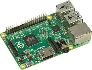
Raspberry-Pi-2-Bare-BR
An ARMv7 was used to power older versions of the popular Raspberry Pi single-board computers like this Raspberry Pi 2 from 2015.
Cubox
An ARMv7 is also used to power the CuBox family of single-board computers.

The 32-bit ARM architecture (ARM32), such as Armv7-A (implementing AArch32; see section on Armv8-A for more on it), was the most widely used architecture in mobile devices as of 2011.

Since 1995, various versions of the ARM Architecture Reference Manual (see § External links) have been the primary source of documentation on the ARM processor architecture and instruction set, distinguishing interfaces that all ARM processors are required to support (such as instruction semantics) from implementation details that may vary. The architecture has evolved over time, and version seven of the architecture, ARMv7, defines three architecture "profiles":

  • A-profile, the "Application" profile, implemented by 32-bit cores in the Cortex-A series and by some non-ARM cores
  • R-profile, the "Real-time" profile, implemented by cores in the Cortex-R series
  • M-profile, the "Microcontroller" profile, implemented by most cores in the Cortex-M series

Although the architecture profiles were first defined for ARMv7, ARM subsequently defined the ARMv6-M architecture (used by the Cortex M0/M0+/M1) as a subset of the ARMv7-M profile with fewer instructions.

CPU modes

Except in the M-profile, the 32-bit ARM architecture specifies several CPU modes, depending on the implemented architecture features. At any moment in time, the CPU can be in only one mode, but it can switch modes due to external events (interrupts) or programmatically.

  • User mode: The only non-privileged mode.
  • FIQ mode: A privileged mode that is entered whenever the processor accepts a fast interrupt request.
  • IRQ mode: A privileged mode that is entered whenever the processor accepts an interrupt.
  • Supervisor (svc) mode: A privileged mode entered whenever the CPU is reset or when an SVC instruction is executed.
  • Abort mode: A privileged mode that is entered whenever a prefetch abort or data abort exception occurs.
  • Undefined mode: A privileged mode that is entered whenever an undefined instruction exception occurs.
  • System mode (ARMv4 and above): The only privileged mode that is not entered by an exception. It can only be entered by executing an instruction that explicitly writes to the mode bits of the Current Program Status Register (CPSR) from another privileged mode (not from user mode).
  • Monitor mode (ARMv6 and ARMv7 Security Extensions, ARMv8 EL3): A monitor mode is introduced to support TrustZone extension in ARM cores.
  • Hyp mode (ARMv7 Virtualization Extensions, ARMv8 EL2): A hypervisor mode that supports Popek and Goldberg virtualization requirements for the non-secure operation of the CPU.
  • Thread mode (ARMv6-M, ARMv7-M, ARMv8-M): A mode which can be specified as either privileged or unprivileged. Whether the Main Stack Pointer (MSP) or Process Stack Pointer (PSP) is used can also be specified in CONTROL register with privileged access. This mode is designed for user tasks in RTOS environment but it's typically used in bare-metal for super-loop.
  • Handler mode (ARMv6-M, ARMv7-M, ARMv8-M): A mode dedicated for exception handling (except the RESET which are handled in Thread mode). Handler mode always uses MSP and works in privileged level.

Instruction set

The original (and subsequent) ARM implementation was hardwired without microcode, like the much simpler 8-bit 6502 processor used in prior Acorn microcomputers.

The 32-bit ARM architecture (and the 64-bit architecture for the most part) includes the following RISC features:

  • Load–store architecture.
  • No support for unaligned memory accesses in the original version of the architecture. ARMv6 and later, except some microcontroller versions, support unaligned accesses for half-word and single-word load/store instructions with some limitations, such as no guaranteed atomicity.
  • Uniform 16 × 32-bit register file (including the program counter, stack pointer and the link register).
  • Fixed instruction width of 32 bits to ease decoding and pipelining, at the cost of decreased code density. Later, the Thumb instruction set added 16-bit instructions and increased code density.
  • Mostly single clock-cycle execution.

To compensate for the simpler design, compared with processors like the Intel 80286 and Motorola 68020, some additional design features were used:

  • Conditional execution of most instructions reduces branch overhead and compensates for the lack of a branch predictor in early chips.
  • Arithmetic instructions alter condition codes only when desired.
  • 32-bit barrel shifter can be used without performance penalty with most arithmetic instructions and address calculations.
  • Has powerful indexed addressing modes.
  • A link register supports fast leaf function calls.
  • A simple, but fast, 2-priority-level interrupt subsystem has switched register banks.

Arithmetic instructions

ARM includes integer arithmetic operations for add, subtract, and multiply; some versions of the architecture also support divide operations.

ARM supports 32-bit × 32-bit multiplies with either a 32-bit result or 64-bit result, though Cortex-M0 / M0+ / M1 cores don't support 64-bit results. Some ARM cores also support 16-bit × 16-bit and 32-bit × 16-bit multiplies.

The divide instructions are only included in the following ARM architectures:

  • Armv7-M and Armv7E-M architectures always include divide instructions.
  • Armv7-R architecture always includes divide instructions in the Thumb instruction set, but optionally in its 32-bit instruction set.
  • Armv7-A architecture optionally includes the divide instructions. The instructions might not be implemented, or implemented only in the Thumb instruction set, or implemented in both the Thumb and ARM instruction sets, or implemented if the Virtualization Extensions are included.

Registers

Registers across CPU modes
usr sys svc abt und irq fiq
R0
R1
R2
R3
R4
R5
R6
R7
R8 R8_fiq
R9 R9_fiq
R10 R10_fiq
R11 R11_fiq
R12 R12_fiq
R13 R13_svc R13_abt R13_und R13_irq R13_fiq
R14 R14_svc R14_abt R14_und R14_irq R14_fiq
R15
CPSR
SPSR_svc SPSR_abt SPSR_und SPSR_irq SPSR_fiq

Registers R0 through R7 are the same across all CPU modes; they are never banked.

Registers R8 through R12 are the same across all CPU modes except FIQ mode. FIQ mode has its own distinct R8 through R12 registers.

R13 and R14 are banked across all privileged CPU modes except system mode. That is, each mode that can be entered because of an exception has its own R13 and R14. These registers generally contain the stack pointer and the return address from function calls, respectively.

Aliases:

  • R13 is also referred to as SP, the stack pointer.
  • R14 is also referred to as LR, the link register.
  • R15 is also referred to as PC, the program counter.

The Current Program Status Register (CPSR) has the following 32 bits.

  • M (bits 0–4) is the processor mode bits.
  • T (bit 5) is the Thumb state bit.
  • F (bit 6) is the FIQ disable bit.
  • I (bit 7) is the IRQ disable bit.
  • A (bit 8) is the imprecise data abort disable bit.
  • E (bit 9) is the data endianness bit.
  • IT (bits 10–15 and 25–26) is the if-then state bits.
  • GE (bits 16–19) is the greater-than-or-equal-to bits.
  • DNM (bits 20–23) is the do not modify bits.
  • J (bit 24) is the Java state bit.
  • Q (bit 27) is the sticky overflow bit.
  • V (bit 28) is the overflow bit.
  • C (bit 29) is the carry/borrow/extend bit.
  • Z (bit 30) is the zero bit.
  • N (bit 31) is the negative/less than bit.

Conditional execution

Almost every ARM instruction has a conditional execution feature called predication, which is implemented with a 4-bit condition code selector (the predicate). To allow for unconditional execution, one of the four-bit codes causes the instruction to be always executed. Most other CPU architectures only have condition codes on branch instructions.

Though the predicate takes up four of the 32 bits in an instruction code, and thus cuts down significantly on the encoding bits available for displacements in memory access instructions, it avoids branch instructions when generating code for small if statements. Apart from eliminating the branch instructions themselves, this preserves the fetch/decode/execute pipeline at the cost of only one cycle per skipped instruction.

An algorithm that provides a good example of conditional execution is the subtraction-based Euclidean algorithm for computing the greatest common divisor. In the C programming language, the algorithm can be written as:

int gcd(int a, int b) {
  while (a != b)  // We enter the loop when a < b or a > b, but not when a == b
    if (a > b)   // When a > b we do this
      a -= b;
    else         // When a < b we do that (no "if (a < b)" needed since a != b is checked in while condition)
      b -= a;
  return a;
}

The same algorithm can be rewritten in a way closer to target ARM instructions as:

loop:
    // Compare a and b
    GT = a > b;
    LT = a < b;
    NE = a != b;

    // Perform operations based on flag results
    if (GT) a -= b;    // Subtract *only* if greater-than
    if (LT) b -= a;    // Subtract *only* if less-than
    if (NE) goto loop; // Loop *only* if compared values were not equal
    return a;

and coded in assembly language as:

; assign a to register r0, b to r1
loop:   CMP    r0, r1       ; set condition "NE" if (a != b),
                            ;               "GT" if (a > b),
                            ;            or "LT" if (a < b)
        SUBGT  r0, r0, r1   ; if "GT" (Greater Than), then a = a - b
        SUBLT  r1, r1, r0   ; if "LT" (Less Than), then b = b - a
        BNE  loop           ; if "NE" (Not Equal), then loop
        B    lr             ; return

which avoids the branches around the then and else clauses. If r0 and r1 are equal then neither of the SUB instructions will be executed, eliminating the need for a conditional branch to implement the while check at the top of the loop, for example had SUBLE (less than or equal) been used.

One of the ways that Thumb code provides a more dense encoding is to remove the four-bit selector from non-branch instructions.

Other features

Another feature of the instruction set is the ability to fold shifts and rotates into the data processing (arithmetic, logical, and register-register move) instructions, so that, for example, the statement in C language:

a += (j << 2);

could be rendered as a one-word, one-cycle instruction:

ADD  Ra, Ra, Rj, LSL #2

This results in the typical ARM program being denser than expected with fewer memory accesses; thus the pipeline is used more efficiently.

The ARM processor also has features rarely seen in other RISC architectures, such as PC-relative addressing (indeed, on the 32-bit ARM the PC is one of its 16 registers) and pre- and post-increment addressing modes.

The ARM instruction set has increased over time. Some early ARM processors (before ARM7TDMI), for example, have no instruction to store a two-byte quantity.

Pipelines and other implementation issues

The ARM7 and earlier implementations have a three-stage pipeline; the stages being fetch, decode, and execute. Higher-performance designs, such as the ARM9, have deeper pipelines: Cortex-A8 has thirteen stages. Additional implementation changes for higher performance include a faster adder and more extensive branch prediction logic. The difference between the ARM7DI and ARM7DMI cores, for example, was an improved multiplier; hence the added "M".

Coprocessors

The ARM architecture (pre-Armv8) provides a non-intrusive way of extending the instruction set using "coprocessors" that can be addressed using MCR, MRC, MRRC, MCRR, and similar instructions. The coprocessor space is divided logically into 16 coprocessors with numbers from 0 to 15, coprocessor 15 (cp15) being reserved for some typical control functions like managing the caches and MMU operation on processors that have one.

In ARM-based machines, peripheral devices are usually attached to the processor by mapping their physical registers into ARM memory space, into the coprocessor space, or by connecting to another device (a bus) that in turn attaches to the processor. Coprocessor accesses have lower latency, so some peripherals—for example, an XScale interrupt controller—are accessible in both ways: through memory and through coprocessors.

In other cases, chip designers only integrate hardware using the coprocessor mechanism. For example, an image processing engine might be a small ARM7TDMI core combined with a coprocessor that has specialised operations to support a specific set of HDTV transcoding primitives.

Debugging

All modern ARM processors include hardware debugging facilities, allowing software debuggers to perform operations such as halting, stepping, and breakpointing of code starting from reset. These facilities are built using JTAG support, though some newer cores optionally support ARM's own two-wire "SWD" protocol. In ARM7TDMI cores, the "D" represented JTAG debug support, and the "I" represented presence of an "EmbeddedICE" debug module. For ARM7 and ARM9 core generations, EmbeddedICE over JTAG was a de facto debug standard, though not architecturally guaranteed.

The ARMv7 architecture defines basic debug facilities at an architectural level. These include breakpoints, watchpoints and instruction execution in a "Debug Mode"; similar facilities were also available with EmbeddedICE. Both "halt mode" and "monitor" mode debugging are supported. The actual transport mechanism used to access the debug facilities is not architecturally specified, but implementations generally include JTAG support.

There is a separate ARM "CoreSight" debug architecture, which is not architecturally required by ARMv7 processors.

Debug Access Port

The Debug Access Port (DAP) is an implementation of an ARM Debug Interface.

There are two different supported implementations, the Serial Wire JTAG Debug Port (SWJ-DP) and the Serial Wire Debug Port (SW-DP). CMSIS-DAP is a standard interface that describes how various debugging software on a host PC can communicate over USB to firmware running on a hardware debugger, which in turn talks over SWD or JTAG to a CoreSight-enabled ARM Cortex CPU.

DSP enhancement instructions

To improve the ARM architecture for digital signal processing and multimedia applications, DSP instructions were added to the set. These are signified by an "E" in the name of the ARMv5TE and ARMv5TEJ architectures. E-variants also imply T, D, M, and I.

The new instructions are common in digital signal processor (DSP) architectures. They include variations on signed multiply–accumulate, saturated add and subtract, and count leading zeros.

SIMD extensions for multimedia

Introduced in the ARMv6 architecture, this was a precursor to Advanced SIMD, also named Neon.

Jazelle

Jazelle DBX (Direct Bytecode eXecution) is a technique that allows Java bytecode to be executed directly in the ARM architecture as a third execution state (and instruction set) alongside the existing ARM and Thumb-mode. Support for this state is signified by the "J" in the ARMv5TEJ architecture, and in ARM9EJ-S and ARM7EJ-S core names. Support for this state is required starting in ARMv6 (except for the ARMv7-M profile), though newer cores only include a trivial implementation that provides no hardware acceleration.

Thumb

To improve compiled code density, processors since the ARM7TDMI (released in 1994) have featured the Thumb instruction set, which have their own state. (The "T" in "TDMI" indicates the Thumb feature.) When in this state, the processor executes the Thumb instruction set, a compact 16-bit encoding for a subset of the ARM instruction set. Most of the Thumb instructions are directly mapped to normal ARM instructions. The space saving comes from making some of the instruction operands implicit and limiting the number of possibilities compared to the ARM instructions executed in the ARM instruction set state.

In Thumb, the 16-bit opcodes have less functionality. For example, only branches can be conditional, and many opcodes are restricted to accessing only half of all of the CPU's general-purpose registers. The shorter opcodes give improved code density overall, even though some operations require extra instructions. In situations where the memory port or bus width is constrained to less than 32 bits, the shorter Thumb opcodes allow increased performance compared with 32-bit ARM code, as less program code may need to be loaded into the processor over the constrained memory bandwidth.

Unlike processor architectures with variable length (16- or 32-bit) instructions, such as the Cray-1 and Hitachi SuperH, the ARM and Thumb instruction sets exist independently of each other. Embedded hardware, such as the Game Boy Advance, typically have a small amount of RAM accessible with a full 32-bit datapath; the majority is accessed via a 16-bit or narrower secondary datapath. In this situation, it usually makes sense to compile Thumb code and hand-optimise a few of the most CPU-intensive sections using full 32-bit ARM instructions, placing these wider instructions into the 32-bit bus accessible memory.

The first processor with a Thumb instruction decoder was the ARM7TDMI. All ARM9 and later families, including XScale, have included a Thumb instruction decoder. It includes instructions adopted from the Hitachi SuperH (1992), which was licensed by ARM. ARM's smallest processor families (Cortex M0 and M1) implement only the 16-bit Thumb instruction set for maximum performance in lowest cost applications.

Thumb-2

Thumb-2 technology was introduced in the ARM1156 core, announced in 2003. Thumb-2 extends the limited 16-bit instruction set of Thumb with additional 32-bit instructions to give the instruction set more breadth, thus producing a variable-length instruction set. A stated aim for Thumb-2 was to achieve code density similar to Thumb with performance similar to the ARM instruction set on 32-bit memory.

Thumb-2 extends the Thumb instruction set with bit-field manipulation, table branches and conditional execution. At the same time, the ARM instruction set was extended to maintain equivalent functionality in both instruction sets. A new "Unified Assembly Language" (UAL) supports generation of either Thumb or ARM instructions from the same source code; versions of Thumb seen on ARMv7 processors are essentially as capable as ARM code (including the ability to write interrupt handlers). This requires a bit of care, and use of a new "IT" (if-then) instruction, which permits up to four successive instructions to execute based on a tested condition, or on its inverse. When compiling into ARM code, this is ignored, but when compiling into Thumb it generates an actual instruction. For example:

; if (r0 == r1)
CMP r0, r1
ITE EQ        ; ARM: no code ... Thumb: IT instruction
; then r0 = r2;
MOVEQ r0, r2  ; ARM: conditional; Thumb: condition via ITE 'T' (then)
; else r0 = r3;
MOVNE r0, r3  ; ARM: conditional; Thumb: condition via ITE 'E' (else)
; recall that the Thumb MOV instruction has no bits to encode "EQ" or "NE".

All ARMv7 chips support the Thumb instruction set. All chips in the Cortex-A series, Cortex-R series, and ARM11 series support both "ARM instruction set state" and "Thumb instruction set state", while chips in the Cortex-M series support only the Thumb instruction set.

Thumb Execution Environment (ThumbEE)

ThumbEE (erroneously called Thumb-2EE in some ARM documentation), which was marketed as Jazelle RCT (Runtime Compilation Target), was announced in 2005 and deprecated in 2011. It first appeared in the Cortex-A8 processor. ThumbEE is a fourth instruction set state, making small changes to the Thumb-2 extended instruction set. These changes make the instruction set particularly suited to code generated at runtime (e.g. by JIT compilation) in managed Execution Environments. ThumbEE is a target for languages such as Java, C#, Perl, and Python, and allows JIT compilers to output smaller compiled code without reducing performance.

New features provided by ThumbEE include automatic null pointer checks on every load and store instruction, an instruction to perform an array bounds check, and special instructions that call a handler. In addition, because it utilises Thumb-2 technology, ThumbEE provides access to registers r8–r15 (where the Jazelle/DBX Java VM state is held). Handlers are small sections of frequently called code, commonly used to implement high level languages, such as allocating memory for a new object. These changes come from repurposing a handful of opcodes, and knowing the core is in the new ThumbEE state.

On 23 November 2011, Arm deprecated any use of the ThumbEE instruction set, and Armv8 removes support for ThumbEE.

Floating-point (VFP)

VFP (Vector Floating Point) technology is a floating-point unit (FPU) coprocessor extension to the ARM architecture (implemented differently in Armv8 – coprocessors not defined there). It provides low-cost single-precision and double-precision floating-point computation fully compliant with the ANSI/IEEE Std 754-1985 Standard for Binary Floating-Point Arithmetic. VFP provides floating-point computation suitable for a wide spectrum of applications such as PDAs, smartphones, voice compression and decompression, three-dimensional graphics and digital audio, printers, set-top boxes, and automotive applications. The VFP architecture was intended to support execution of short "vector mode" instructions but these operated on each vector element sequentially and thus did not offer the performance of true single instruction, multiple data (SIMD) vector parallelism. This vector mode was therefore removed shortly after its introduction, to be replaced with the much more powerful Advanced SIMD, also named Neon.

Some devices such as the ARM Cortex-A8 have a cut-down VFPLite module instead of a full VFP module, and require roughly ten times more clock cycles per float operation. Pre-Armv8 architecture implemented floating-point/SIMD with the coprocessor interface. Other floating-point and/or SIMD units found in ARM-based processors using the coprocessor interface include FPA, FPE, iwMMXt, some of which were implemented in software by trapping but could have been implemented in hardware. They provide some of the same functionality as VFP but are not opcode-compatible with it. FPA10 also provides extended precision, but implements correct rounding (required by IEEE 754) only in single precision.

VFPv1
Obsolete
VFPv2
An optional extension to the ARM instruction set in the ARMv5TE, ARMv5TEJ and ARMv6 architectures. VFPv2 has 16 64-bit FPU registers.
VFPv3 or VFPv3-D32
Implemented on most Cortex-A8 and A9 ARMv7 processors. It is backward-compatible with VFPv2, except that it cannot trap floating-point exceptions. VFPv3 has 32 64-bit FPU registers as standard, adds VCVT instructions to convert between scalar, float and double, adds immediate mode to VMOV such that constants can be loaded into FPU registers.
VFPv3-D16
As above, but with only 16 64-bit FPU registers. Implemented on Cortex-R4 and R5 processors and the Tegra 2 (Cortex-A9).
VFPv3-F16
Uncommon; it supports IEEE754-2008 half-precision (16-bit) floating point as a storage format.
VFPv4 or VFPv4-D32
Implemented on Cortex-A12 and A15 ARMv7 processors, Cortex-A7 optionally has VFPv4-D32 in the case of an FPU with Neon. VFPv4 has 32 64-bit FPU registers as standard, adds both half-precision support as a storage format and fused multiply-accumulate instructions to the features of VFPv3.
VFPv4-D16
As above, but it has only 16 64-bit FPU registers. Implemented on Cortex-A5 and A7 processors in the case of an FPU without Neon.
VFPv5-D16-M
Implemented on Cortex-M7 when single and double-precision floating-point core option exists.

In Debian Linux and derivatives such as Ubuntu and Linux Mint, armhf (ARM hard float) refers to the ARMv7 architecture including the additional VFP3-D16 floating-point hardware extension (and Thumb-2) above. Software packages and cross-compiler tools use the armhf vs. arm/armel suffixes to differentiate.

Advanced SIMD (Neon)

The Advanced SIMD extension (also known as Neon or "MPE" Media Processing Engine) is a combined 64- and 128-bit SIMD instruction set that provides standardised acceleration for media and signal processing applications. Neon is included in all Cortex-A8 devices, but is optional in Cortex-A9 devices. Neon can execute MP3 audio decoding on CPUs running at 10 MHz, and can run the GSM adaptive multi-rate (AMR) speech codec at 13 MHz. It features a comprehensive instruction set, separate register files, and independent execution hardware. Neon supports 8-, 16-, 32-, and 64-bit integer and single-precision (32-bit) floating-point data and SIMD operations for handling audio and video processing as well as graphics and gaming processing. In Neon, the SIMD supports up to 16 operations at the same time. The Neon hardware shares the same floating-point registers as used in VFP. Devices such as the ARM Cortex-A8 and Cortex-A9 support 128-bit vectors, but will execute with 64 bits at a time, whereas newer Cortex-A15 devices can execute 128 bits at a time.

A quirk of Neon in Armv7 devices is that it flushes all subnormal numbers to zero, and as a result the GCC compiler will not use it unless -funsafe-math-optimizations, which allows losing denormals, is turned on. "Enhanced" Neon defined since Armv8 does not have this quirk, but as of GCC 8.2 the same flag is still required to enable Neon instructions. On the other hand, GCC does consider Neon safe on AArch64 for Armv8.

ProjectNe10 is ARM's first open-source project (from its inception; while they acquired an older project, now named Mbed TLS). The Ne10 library is a set of common, useful functions written in both Neon and C (for compatibility). The library was created to allow developers to use Neon optimisations without learning Neon, but it also serves as a set of highly optimised Neon intrinsic and assembly code examples for common DSP, arithmetic, and image processing routines. The source code is available on GitHub.

ARM Helium technology

Helium is the M-Profile Vector Extension (MVE). It adds more than 150 scalar and vector instructions.

Security extensions

TrustZone (for Cortex-A profile)

The Security Extensions, marketed as TrustZone Technology, is in ARMv6KZ and later application profile architectures. It provides a low-cost alternative to adding another dedicated security core to an SoC, by providing two virtual processors backed by hardware based access control. This lets the application core switch between two states, referred to as worlds (to reduce confusion with other names for capability domains), to prevent information leaking from the more trusted world to the less trusted world. This world switch is generally orthogonal to all other capabilities of the processor, thus each world can operate independently of the other while using the same core. Memory and peripherals are then made aware of the operating world of the core and may use this to provide access control to secrets and code on the device.

Typically, a rich operating system is run in the less trusted world, with smaller security-specialised code in the more trusted world, aiming to reduce the attack surface. Typical applications include DRM functionality for controlling the use of media on ARM-based devices, and preventing any unapproved use of the device.

In practice, since the specific implementation details of proprietary TrustZone implementations have not been publicly disclosed for review, it is unclear what level of assurance is provided for a given threat model, but they are not immune from attack.

Open Virtualization is an open source implementation of the trusted world architecture for TrustZone.

AMD has licensed and incorporated TrustZone technology into its Secure Processor Technology. Enabled in some but not all products, AMD's APUs include a Cortex-A5 processor for handling secure processing. In fact, the Cortex-A5 TrustZone core had been included in earlier AMD products, but was not enabled due to time constraints.

Samsung Knox uses TrustZone for purposes such as detecting modifications to the kernel, storing certificates and attestating keys.

TrustZone for Armv8-M (for Cortex-M profile)

The Security Extension, marketed as TrustZone for Armv8-M Technology, was introduced in the Armv8-M architecture. While containing similar concepts to TrustZone for Armv8-A, it has a different architectural design, as world switching is performed using branch instructions instead of using exceptions. It also supports safe interleaved interrupt handling from either world regardless of the current security state. Together these features provide low latency calls to the secure world and responsive interrupt handling. ARM provides a reference stack of secure world code in the form of Trusted Firmware for M and PSA Certified.

No-execute page protection

As of ARMv6, the ARM architecture supports no-execute page protection, which is referred to as XN, for eXecute Never.

Large Physical Address Extension (LPAE)

The Large Physical Address Extension (LPAE), which extends the physical address size from 32 bits to 40 bits, was added to the Armv7-A architecture in 2011.

The physical address size may be even larger in processors based on the 64-bit (Armv8-A) architecture. For example, it is 44 bits in Cortex-A75 and Cortex-A65AE.

Armv8-R and Armv8-M

The Armv8-R and Armv8-M architectures, announced after the Armv8-A architecture, share some features with Armv8-A. However, Armv8-M does not include any 64-bit AArch64 instructions, and Armv8-R originally did not include any AArch64 instructions; those instructions were added to Armv8-R later.

Armv8.1-M

The Armv8.1-M architecture, announced in February 2019, is an enhancement of the Armv8-M architecture. It brings new features including:

  • A new vector instruction set extension. The M-Profile Vector Extension (MVE), or Helium, is for signal processing and machine learning applications.
  • Additional instruction set enhancements for loops and branches (Low Overhead Branch Extension).
  • Instructions for half-precision floating-point support.
  • Instruction set enhancement for TrustZone management for Floating Point Unit (FPU).
  • New memory attribute in the Memory Protection Unit (MPU).
  • Enhancements in debug including Performance Monitoring Unit (PMU), Unprivileged Debug Extension, and additional debug support focus on signal processing application developments.
  • Reliability, Availability and Serviceability (RAS) extension.

64/32-bit architecture

ARMCortexA57A53
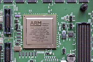
Armv8-A Platform with Cortex A57/A53 MPCore big.LITTLE CPU chip

Armv8

Armv8-A

Announced in October 2011, Armv8-A (often called ARMv8 while the Armv8-R is also available) represents a fundamental change to the ARM architecture. It adds an optional 64-bit architecture named "AArch64" and the associated new "A64" instruction set. AArch64 provides user-space compatibility with Armv7-A, the 32-bit architecture, therein referred to as "AArch32" and the old 32-bit instruction set, now named "A32". The Thumb instruction set is referred to as "T32" and has no 64-bit counterpart. Armv8-A allows 32-bit applications to be executed in a 64-bit OS, and a 32-bit OS to be under the control of a 64-bit hypervisor. ARM announced their Cortex-A53 and Cortex-A57 cores on 30 October 2012. Apple was the first to release an Armv8-A compatible core in a consumer product (Apple A7 in iPhone 5S). AppliedMicro, using an FPGA, was the first to demo Armv8-A. The first Armv8-A SoC from Samsung is the Exynos 5433 used in the Galaxy Note 4, which features two clusters of four Cortex-A57 and Cortex-A53 cores in a big.LITTLE configuration; but it will run only in AArch32 mode.

To both AArch32 and AArch64, Armv8-A makes VFPv3/v4 and advanced SIMD (Neon) standard. It also adds cryptography instructions supporting AES, SHA-1/SHA-256 and finite field arithmetic. AArch64 was introduced in Armv8-A and its subsequent revision. AArch64 is not included in the 32-bit Armv8-R and Armv8-M architectures.

Armv8-R

Optional AArch64 support was added to the Armv8-R profile, with the first ARM core implementing it being the Cortex-R82. It adds the A64 instruction set.

Armv9

Armv9-A

Announced in March 2021, the updated architecture places a focus on secure execution and compartmentalisation.

Arm SystemReady

Arm SystemReady, formerly named Arm ServerReady, is a certification program that helps land the generic off-the-shelf operating systems and hypervisors on to the Arm-based systems from datacenter servers to industrial edge and IoT devices. The key building blocks of the program are the specifications for minimum hardware and firmware requirements that the operating systems and hypervisors can rely upon. These specifications are:

  • Base System Architecture (BSA) and the market segment specific supplements (e.g., Server BSA supplement)
  • Base Boot Requirements (BBR) and Base Boot Security Requirements (BBR)

These specifications are co-developed by Arm and its partners in the System Architecture Advisory Committee (SystemArchAC).

Architecture Compliance Suite (ACS) is the test tools that help to check the compliance of these specifications. The Arm SystemReady Requirements Specification documents the requirements of the certifications.

This program was introduced by Arm in 2020 at the first DevSummit event. Its predecessor Arm ServerReady was introduced in 2018 at the Arm TechCon event. This program currently includes four bands:

  • SystemReady SR: this band is for servers that support operating systems and hypervisors that expect UEFI, ACPI and SMBIOS interfaces.
  • SystemReady LS: this band is for servers that hyperscalers use to support Linux operating systems that expect LinuxBoot firmware along with the ACPI and SMBIOS interfaces.
  • SystemReady ES: this band is for the industrial edge and IoT devices that support operating systems and hypervisors that expect UEFI, ACPI and SMBIOS interfaces.
  • SystemReady IR: this band is for the industrial edge and IoT devices that support operating systems that expect UEFI and devicetree interfaces.

PSA Certified

PSA Certified, formerly named Platform Security Architecture, is an architecture-agnostic security framework and evaluation scheme. It is intended to help secure Internet of Things (IoT) devices built on system-on-a-chip (SoC) processors. It was introduced to increase security where a full trusted execution environment is too large or complex.

The architecture was introduced by Arm in 2017 at the annual TechCon event. Although the scheme is architecture agnostic, it was first implemented on Arm Cortex-M processor cores intended for microcontroller use. PSA Certified includes freely available threat models and security analyses that demonstrate the process for deciding on security features in common IoT products. It also provides freely downloadable application programming interface (API) packages, architectural specifications, open-source firmware implementations, and related test suites.

Following the development of the architecture security framework in 2017, the PSA Certified assurance scheme launched two years later at Embedded World in 2019. PSA Certified offers a multi-level security evaluation scheme for chip vendors, OS providers and IoT device makers. The Embedded World presentation introduced chip vendors to Level 1 Certification. A draft of Level 2 protection was presented at the same time. Level 2 certification became a usable standard in February 2020.

The certification was created by PSA Joint Stakeholders to enable a security-by-design approach for a diverse set of IoT products. PSA Certified specifications are implementation and architecture agnostic, as a result they can be applied to any chip, software or device. The certification also removes industry fragmentation for IoT product manufacturers and developers.

Operating system support

32-bit operating systems

Historical operating systems

The first 32-bit ARM-based personal computer, the Acorn Archimedes, was originally intended to run an ambitious operating system called ARX. The machines shipped with RISC OS which was also used on later ARM-based systems from Acorn and other vendors. Some early Acorn machines were also able to run a Unix port called RISC iX. (Neither is to be confused with RISC/os, a contemporary Unix variant for the MIPS architecture.)

Embedded operating systems

The 32-bit ARM architecture is supported by a large number of embedded and real-time operating systems, including:

  • A2
  • Android
  • ChibiOS/RT
  • Deos
  • DRYOS
  • eCos
  • embOS
  • FreeBSD
  • FreeRTOS
  • INTEGRITY
  • Linux
  • Micro-Controller Operating Systems
  • Mbed
  • MINIX 3
  • MQX
  • Nucleus PLUS
  • NuttX
  • Operating System Embedded (OSE)
  • OS-9
  • Pharos
  • Plan 9
  • PikeOS
  • QNX
  • RIOT
  • RTEMS
  • RTXC Quadros
  • SCIOPTA
  • ThreadX
  • TizenRT
  • T-Kernel
  • VxWorks
  • Windows Embedded Compact
  • Windows 10 IoT Core
  • Zephyr

Mobile device operating systems

The 32-bit ARM architecture is the primary hardware environment for most mobile device operating systems such as:

  • Android
  • BlackBerry OS/BlackBerry 10
  • ChromeOS
  • Mobian
  • Sailfish
  • postmarketOS
  • Tizen
  • Ubuntu Touch
  • webOS

Formerly, but now discontinued:

Desktop and server operating systems

The 32-bit ARM architecture is supported by RISC OS and by multiple Unix-like operating systems including:

64-bit operating systems

Embedded operating systems

  • INTEGRITY
  • OSE
  • SCIOPTA
  • seL4
  • Pharos
  • FreeRTOS
  • QNX
  • Zephyr

Mobile device operating systems

  • Android supports Armv8-A in Android Lollipop (5.0) and later.
  • iOS supports Armv8-A in iOS 7 and later on 64-bit Apple SoCs. iOS 11 and later, and iPadOS, only support 64-bit ARM processors and applications.
  • Mobian
  • PostmarketOS
  • Arch Linux ARM
  • Manjaro

Desktop and server operating systems

  • Support for Armv8-A was merged into the Linux kernel version 3.7 in late 2012. Armv8-A is supported by a number of Linux distributions, such as:
  • Support for Armv8-A was merged into FreeBSD in late 2014.
  • OpenBSD has Armv8 support as of 2017.
  • NetBSD has Armv8 support as of early 2018.
  • Windows - Windows 10 runs 32-bit "x86 and 32-bit ARM applications", as well as native ARM64 desktop apps; Windows 11 does so as well. Support for 64-bit ARM apps in the Microsoft Store has been available since November 2018.
  • macOS has ARM support starting with macOS Big Sur as of late 2020. Rosetta 2 adds support for x86-64 applications but not virtualization of x86-64 computer platforms.

Porting to 32- or 64-bit ARM operating systems

Windows applications recompiled for ARM and linked with Winelib, from the Wine project, can run on 32-bit or 64-bit ARM in Linux, FreeBSD, or other compatible operating systems. x86 binaries, e.g. when not specially compiled for ARM, have been demonstrated on ARM using QEMU with Wine (on Linux and more), but do not work at full speed or same capability as with Winelib.

See also

Kids robot.svg In Spanish: Arquitectura ARM para niños

kids search engine
ARM architecture family Facts for Kids. Kiddle Encyclopedia.